pcba-zl

pcb Panelization

PCB Panelization: Design Guidelines, Layout Methods & Cost Optimization

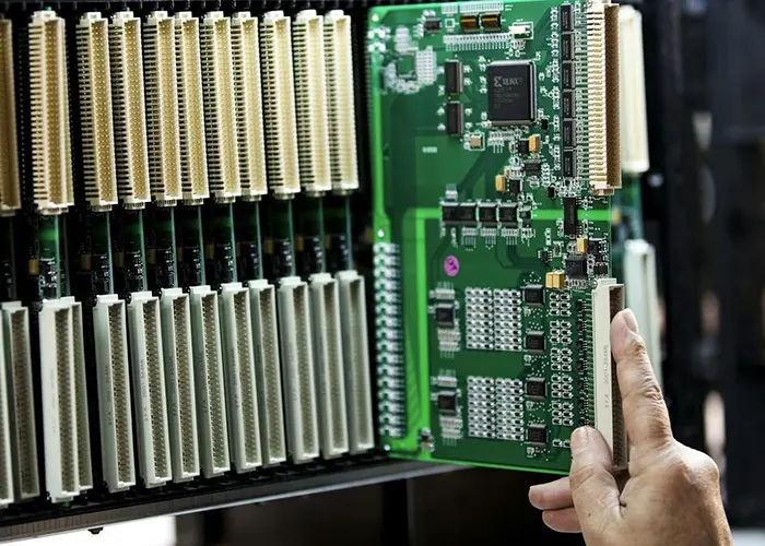
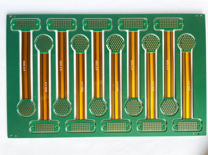
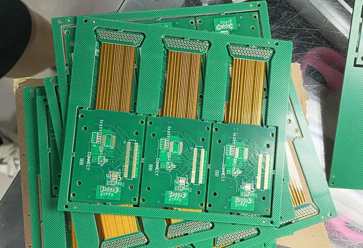
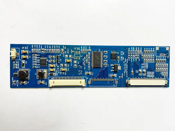
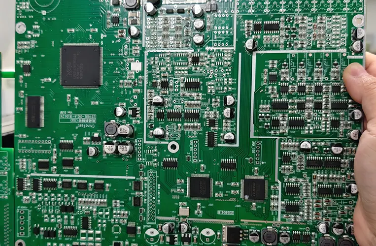
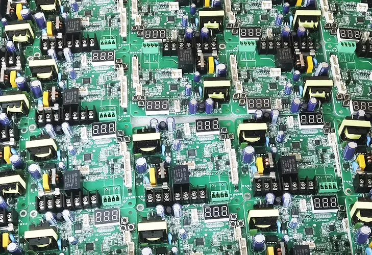
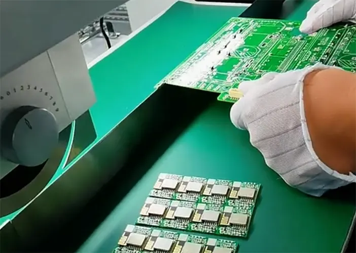
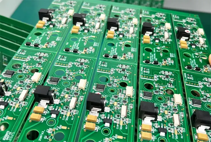
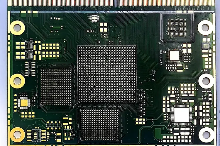
Panelization is a critical step in PCB design that directly affects manufacturability, material utilization, and production cost. It involves combining multiple PCBs into a single panel to meet the size requirements of production equipment, reduce material waste, and improve processing efficiency.
pcb

Optimizing PCB Cavity Design for Reliable Gold/Nickel Plating and COB Packaging

Image sensing technology is widely applied across diverse scenarios such as medical, industrial control, and automotive fields. As image sensors evolve toward thinner, lighter, and smaller components, the design requirement for embedding sensing chips and active or passive electronic components into printed circuit boards (PCBs) has emerged.

Scroll to Top