As server signal rates have surged from 10 Gbps to 112 Gbps and even 224 Gbps (e.g., in AI servers and 1.6T optical module applications), via stubs have become a critical bottleneck limiting signal integrity.
As the core method for eliminating the stub effect, the precision of the back-drilling process directly determines the quality of high-speed signal transmission.
This article provides an overview of methods for precise control and inspection techniques for stubs from a manufacturing perspective.
Origin and Hazards of Stubs
What Is a Stub?
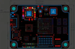
In multi-layer server PCBs (typically 12 layers or more, commonly 16–24 layers), signals often transition from the top layer to an inner layer (e.g., from L1 to L6) using a plated through-hole (PTH).
The portion of the via extending beyond Layer 6 down to the bottom consists of unused copper and does not carry any signal.
Engineers refer to this excess copper wall as a “stub,” and it can extend up to several millimeters in length.
As shown in the diagram below:

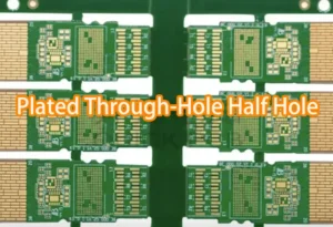
Note: Technicians perform the back-drilling on the back side of the PCB.
They use a larger-diameter drill bit to drill upward from the bottom, precisely removing the stub section.
The Three Major Hazards of Stubs to High-Speed Signals
1. Quarter-Wavelength Resonance Effect
A stub is essentially a section of transmission line with an open end.
When the stub’s length is exactly one-quarter of the signal’s wavelength, it creates a point of extremely low impedance.
Like a “black hole,” this point “sucks in” signals of specific frequencies from the main transmission line and reflects them back, causing severe insertion loss and forming a “resonance dip” in the frequency domain.
Taking FR-4 board material as an example (DK ≈ 4.0–4.5), a 0.5mm stub will resonate around 10–12 GHz, which falls precisely within the Nyquist bandwidth of many 25 Gbps channels.
2. Impedance Step
Stubs introduce parasitic capacitance (approximately 0.5–1 pF per millimeter) and parasitic inductance (approximately 0.3–0.5 nH per millimeter).
This causes the via impedance to deviate from the designed value.
For example, a 100 Ω differential impedance may drop abruptly to 70–80 Ω, which can trigger signal reflections and deterministic jitter.
3. Electromagnetic Interference Radiation
Unmitigated stubs act as “unintended antennas” that radiate electromagnetic energy outward, potentially causing the product to fail compliance testing.
Relationship Between Data Rate and Stub Tolerance Length
As signal data rates increase, the requirements for stub length become exponentially stricter.
Typical tolerance thresholds for different data rates are shown below:
- <1 Gbps — stub < 1.5 mm ±15%
- 10 Gbps — stub < 0.8 mm ±10%
- 25 Gbps — stub < 0.5 mm ±7%
- 56Gbps — stub < 0.3 mm ±5% 800G optical modules
- 112Gbps — stub < 0.2 mm ±3% AI servers/1.6T optical modules
- 224Gbps — stub < 0.1 mm ±2% Next-generation communication equipment
Precision Control Methods for Back-Drilled Stubs
Key Factors Affecting Stub Control Precision
On the manufacturing side, controlling stub length presents four core challenges:
1. Sheet Thickness Uniformity
Large thickness variations across layers (±0.1 mm) can lead to inaccurate Z-axis compensation.
To prevent this, engineers must control core material and PP (prepreg) thickness tolerances within ±0.05 mm.
2. Drilling Accuracy
Drill bit wear reduces the stability of both hole diameter and drilling depth.
To maintain precision, engineers use diamond-coated drill bits with a service life of at least 2,000 holes.
3. Layer Alignment
Asymmetrical layering results in a lack of reference for depth control;
Engineers design the layer stack to be symmetrical and reserve an 8–10 mil safety margin above the target layer.
4. Depth Control
Three-level machine calibration + real-time board thickness measurement compensation.
Key Process Measures for Precise Depth Control
1. Back Drilling Depth Calculation Formula
Back drilling depth is the core parameter for controlling residual stubs. The calculation formula is:
Back drilling depth = Total board thickness – Distance from the target layer to the drill entry surface + Compensation value
2. CCD Vision Positioning System
High-precision back drilling requires the use of a CCD drilling machine.
The vision positioning system identifies PCB positional deviations in real time (with positioning accuracy within ±5 μm), driving the mechanical structure to dynamically compensate for these deviations.
This resolves the issue of hole misalignment caused by PCB warping and loading errors in traditional mechanical positioning systems.
3. Three-Level Depth Calibration System
Start-up Calibration — Calibrate the Z-axis to ±0.02 mm using a standard-thickness test board.
Per-Board Compensation — Measure the thickness of each individual board with a laser before processing and adjust the drilling depth in real time to eliminate variations in board thickness.
Mid-Process Reinspection — Randomly select 2 boards out of every 50 processed for depth inspection;
Immediately stop the machine if the deviation exceeds ±0.03 mm.
4. Electrical Detection-Based Depth Control Technology
In addition to mechanical depth control, a more advanced solution employs electrical detection for depth control.
This method utilizes the conductivity of the copper layer to automatically stop the drill, enabling zero-stump depth control.
However, this requires higher-specification equipment and is suitable for ultra-high-speed PCBs (112G and above) that demand the utmost signal integrity.
Design Specifications for Back Drilling Diameter and Spacing

Testing Methods for Stub Length
Measuring stub length is a critical step in the closed-loop control of the back-drilling process.
Currently, the industry commonly employs the following three testing methods:
Metallographic Section Analysis (Destructive Testing)
Principle: A PCB sample is cut along the center of the back-drilled hole.
After being embedded in resin, ground, and polished, the stub height is measured directly under a metallographic microscope.
Advantages: Intuitive and accurate; considered the “gold standard” for stub length measurement
Disadvantages: Destructive; only allows for sampling; not suitable for full batch inspection
This method is suitable for first-article verification, process capability assessment, and failure analysis, with a measurement accuracy of up to ±5 μm

TDR Testing Method (Non-Destructive)
Principle: A fast-rising-edge pulse signal is sent to the PCB transmission line.
When a signal encounters a stub during transmission, it generates a reflected wave due to the impedance discontinuity.
Engineers determine the stub location by measuring the time delay of the reflected signal, and they calculate the stub length from this delay.
Advantages: Non-destructive, intuitive and fast, allows for precise localization
Disadvantages: Requires specialized equipment and test fixtures
This method is suitable for in-line batch inspection and impedance consistency verification.
Refer to standards IPC-2141A/IPC-TM-650 2.5.5.7
Network Analyzer Testing Method
Principle: Engineers use a vector network analyzer (VNA) to measure S11 (reflection coefficient) and S21 (transmission coefficient).
They then back-calculate the impedance to determine the length of the residual stub.
When the residual stump exceeds 5 mils (0.127 mm), the reflection coefficient S11 increases significantly (>15 dB).
There is a “threshold” for stub length—at approximately 0.1 mm, reflection deteriorates sharply, with S11 dropping abruptly from -22 dB to -14 dB, exceeding the design threshold of -15 dB.
This means that for high-speed server signals, the stub must be controlled within 0.1 mm (4 mil) to meet the signal integrity requirements for 25 Gbps and above.
For ultra-high-speed applications such as 112G PAM4, where signal-to-noise margins are extremely tight, even minor stub deviations can cause eye closure and packet loss.
Some PCB manufacturers have already achieved consistent control of stub length within 0.1 mm (4 mil).
Controlling residual stubs in server PCB back-drilled holes is a systematic engineering process.
It requires a complete closed-loop system spanning multiple stages.
These include the design stage (layer matching and hole size specifications), the manufacturing process (CCD positioning, three-level depth calibration, and drill bit life management), and quality inspection (metallographic cross-sections and TDR testing).
In the era of 112G and higher-speed AI servers, PCBs are no longer merely carriers of conductors;
Certain products require precise control of microscopic gaps as small as 0.1mm, as this 0.1mm is precisely what determines the success or failure of signal integrity.
Conclusion
As server architectures evolve toward 112G, 224G, AI computing, and 1.6T optical interconnects, the tolerance for signal integrity degradation continues to shrink.
What was once considered a minor manufacturing detail—a residual via stub—has become a critical factor affecting channel performance, insertion loss, return loss, jitter, and overall system reliability.
Effective stub control is no longer achieved through back drilling alone.
Achieving precise stub control demands a coordinated engineering strategy that combines optimized PCB stack-up design, accurate depth calculations, high-precision CCD positioning, real-time thickness compensation, disciplined drill bit management, and comprehensive inspection techniques including metallographic analysis, TDR testing, and VNA verification.
For next-generation high-speed PCBs, controlling residual stub length within 0.1 mm (4 mil) or less has become an essential requirement rather than a manufacturing target.
As signaling speeds continue to increase, even smaller residual stubs will have measurable impacts on signal quality.
Ultimately, successful high-speed PCB manufacturing depends on establishing a complete closed-loop control system that connects design, fabrication, and verification.
Only through precise and consistent stub management can PCB manufacturers deliver the signal integrity, reliability, and performance demanded by modern AI servers, high-performance computing platforms, and future ultra-high-speed communication systems.