Immersion gold and electroplated gold are commonly used processes in today’s printed circuit board (PCB) manufacturing. Many people are unable to correctly distinguish between the two, and some even believe there is no difference between them—a view that is entirely incorrect and must be corrected promptly.
People typically opt for gold plating, but what exactly is gold plating?
When we refer to full-board gold plating, we generally mean “electrolytic gold plating,” “electrolytic nickel-gold plating,” “electrolytic gold,” “electrolytic gold plating,” or “electrolytic nickel-gold plating.”
There is a distinction between soft gold and hard gold (hard gold is generally used for gold fingers).
The process involves dissolving nickel and gold (commonly known as gold salt) in a chemical solution.
The PCB is immersed in the plating tank, and an electric current is applied to deposit a nickel-gold plating layer onto the copper foil surface of the board.
Due to its high hardness, wear resistance, and resistance to oxidation, electroplated nickel-gold is widely used in electronic products.
So what is electroless gold plating? Electroless gold plating involves using a chemical redox reaction to form a plating layer, which is generally thicker.
It is a method of chemical nickel-gold plating that can achieve a thicker gold layer.
Electrolytic Gold Plating vs. Immersion Gold Plating
In fact, there are two types of gold plating processes: one is electroplating, and the other is immersion gold plating.
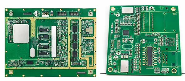
When it comes to gold plating, the solderability is significantly reduced, whereas electroless gold plating offers better solderability; unless the manufacturer specifically requires soldering, most manufacturers now opt for the electroless gold plating process!
Generally, common PCB surface treatments include the following: gold plating (electrolytic gold, electroless gold), silver plating, OSP, and tin spraying (lead-free and leaded).
These are primarily applicable to board materials such as FR-4 or CEM-3; paper-based substrates also have rosin-coated surface treatments.
Regarding poor solderability (inadequate solder uptake), if we rule out causes related to the production and material processes of the SMT manufacturer—such as solder paste—and focus solely on the PCB itself, there are several possible reasons:
1. During PCB printing, is there an oil film on the PAN area? This can hinder solder uptake; a solder wetting test can be performed to verify this.
2. Whether the wetting area of the PAN pad meets design requirements—that is, whether the pad design adequately ensures support for the component.
3. Whether the pad is contaminated; this can be determined through ion contamination testing.
The above three points are essentially the key areas of focus for PCB manufacturers.
As for the advantages and disadvantages of the various surface treatment methods, each has its own strengths and weaknesses!
Gold plating allows PCBs to be stored for a longer period and is less affected by changes in ambient temperature and humidity (compared to other surface treatments);
They can generally be stored for about one year. Tin plating comes next, followed by OSP; for these two surface treatments, special attention must be paid to storage duration under varying environmental conditions.
Generally speaking, electroless silver plating is somewhat different; it is more expensive and requires stricter storage conditions, including packaging in sulfur-free paper, with a shelf life of about three months.
In terms of solderability, electroless gold plating, OSP, and spray tin plating are actually quite similar; manufacturers primarily consider cost-effectiveness when making their decisions!
Difference Between Immersion Gold and Electroplated Gold PCBs
Differences
1. Generally, the gold layer in immersion gold is much thicker than that in electroplated gold. Immersion gold has a golden-yellow appearance, which is more yellow than electroplated gold; based on the surface appearance, customers tend to prefer immersion gold.
The crystal structures formed by these two processes are different.
2. Because the crystal structures formed by electroless gold plating and electroplated gold plating are different, electroless gold plating is easier to solder than electroplated gold plating and does not cause soldering defects that could lead to customer complaints.
At the same time, precisely because electroless gold plating is softer than electroplated gold plating, gold-finger boards generally opt for electroplated gold plating, as hard gold is more wear-resistant.
3. On electroless gold-plated boards, nickel-gold is present only on the pads;
Signal transmission occurs in the copper layer due to the skin effect, so it does not affect the signal.
4. Compared to gold plating, electroless gold has a denser crystal structure and is less prone to oxidation.
5. As routing becomes increasingly dense, line widths and spacing have reached 3–4 mils.
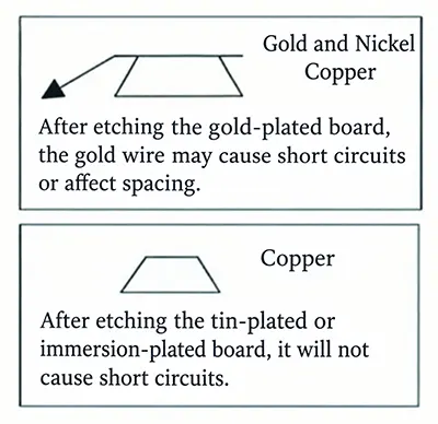
Gold plating is prone to gold-to-gold short circuits. Since electroless gold boards only have nickel-gold on the pads, they do not cause gold-to-gold short circuits.
6. Since nickel-gold plating is applied only to the pads on immersion gold boards, the solder mask adheres more firmly to the copper layer.
This ensures that spacing is not affected when compensation adjustments are made during the manufacturing process.
7. Immersion gold is generally used for boards with relatively high requirements, particularly those needing excellent flatness.
It typically does not exhibit the “black pad” phenomenon after assembly.
The flatness and service life of immersion gold boards are as good as those of gold-plated boards.
These are the differences between immersion gold and electroplated gold boards.
With the current high price of gold on the market, many manufacturers are unwilling to produce electroplated gold boards to save costs and instead produce immersion gold boards with nickel-gold plating only on the pads, which are indeed significantly cheaper.
Note
1. “Immersion gold” and “chemical gold” boards refer to the same type of product, as do “electrolytic gold” and “flash gold” boards.
These are simply different terms used by different groups within the PCB industry.
“Immersion gold” and “electrolytic gold” are more commonly used by peers in mainland China, while “chemical gold” and “flash gold” are more commonly used by peers in Taiwan.
2. The more formal terms for “immersion gold boards” and “chemical gold boards” are “chemical nickel-gold boards” or “chemical nickel-immersion gold boards,” where the nickel/gold layers are deposited using a chemical plating process;
The more formal terms for “electrolytic gold boards” and “flash gold boards” are “electrolytic nickel-gold boards” or “flash-plated gold boards,” where the nickel/gold layers are deposited using a direct current (DC) electroplating process.
3. Refer to the table below for the differences in the mechanisms between chemically nickel-gold-plated boards (deposited gold) and electroplated nickel-gold-plated boards (plated gold):
| Item | ENIG (Electroless Nickel Immersion Gold) | Electroplated Gold |
|---|---|---|
| Process | A phosphorus-containing electroless nickel layer is first deposited onto the bare copper surface of the PCB. The nickel layer contains approximately 7–9% phosphorus and has a thickness of about 3–5 μm. A pure gold layer is then deposited onto the nickel surface by immersion plating, with a thickness of approximately 0.05–0.15 μm. | Copper, nickel, and gold layers are electroplated onto the bare copper surface of the PCB. The nickel layer is approximately 4–8 μm thick, while the gold layer is approximately 1–3 μm thick. |
| Nickel Layer Thickness | 3–5 μm | 4–8 μm |
| Gold Layer Thickness | 0.05–0.15 μm | 1–3 μm |
| Nickel Composition | Contains 7–9% phosphorus | Pure electroplated nickel |
| Gold Type | Immersion gold | Electroplated gold |
Differences in characteristics between ENIG (Electroless Nickel Immersion Gold) boards and gold-plated boards:
| Performance | Electroplated Gold PCB | ENIG PCB |
|---|---|---|
| Appearance | Whitish gold color | Golden yellow |
| Solderability | Generally acceptable, but occasional poor solder joints may occur | Good |
| Signal Transmission | The skin effect can adversely affect high-frequency signal transmission | The skin effect has little impact on signal transmission |
| Quality | 1. Gold surface is prone to oxidation.2. May cause gold-wire micro-shorts.3. Relatively weak solder-mask adhesion | 1. Less prone to oxidation.2. Does not produce gold-wire micro-shorts.3. Provides very good adhesion between the solder mask and PCB surface |
| Engineering | Trace-width compensation may affect spacing | Trace-width compensation does not affect spacing |
Why Isn’t “Tin Spraying” Generally Used?
As ICs become increasingly integrated, they feature more and more densely packed pins.
The vertical tin-spraying process makes it difficult to ensure the pads are perfectly flat, which complicates the SMT placement process; furthermore, the shelf life of tin-sprayed boards is very short.
Gold-plated boards, on the other hand, effectively solve these problems:
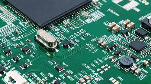
1. In surface-mount technology (SMT), particularly for ultra-small 0603 and 0402 components, the flatness of the pads directly affects the quality of the solder paste printing process and has a decisive impact on the quality of subsequent reflow soldering.
Therefore, full-board gold plating is commonly used in high-density and ultra-small SMT processes.
2. During the prototyping phase, due to factors such as component procurement, boards are often not soldered immediately upon arrival; instead, they are frequently set aside for several weeks or even a month or so before use.
Gold-plated boards have a shelf life many times longer than lead-tin alloy boards, which is why they are widely preferred.
Furthermore, the cost of gold-plated PCBs during the prototyping stage is virtually the same as that of lead-tin alloy boards.
However, as circuit density continues to increase, trace widths and spacing have reached 3–4 mils. This has led to the problem of gold wire short circuits.
As signal frequencies increase, the impact of signal propagation through multilayer coatings due to the skin effect becomes increasingly significant on signal quality.
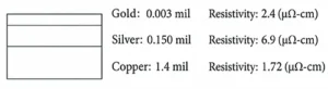
The skin effect refers to the phenomenon in which, in high-frequency alternating current, the current tends to flow concentrated on the surface of a conductor.
According to calculations, the skin depth is related to frequency.
| Frequency (Hz) | Depth (mil) | Frequency (Hz) | Depth (mil) | Frequency (Hz) | Depth (mil) |
|---|---|---|---|---|---|
| 60 | 8.6 | 100 | 6.6 | 1k | 2.1 |
| 10k | 0.66 | 100k | 0.21 | 1M | 0.066 |
| 10M | 0.021 | 100M | 0.0066 | 1G | 0.0021 |