
Millimeter-wave radar circuit boards are the core components of automotive radar systems. They integrate RF circuits, digital signal processing, and power management modules, and are responsible for the transmission, reception, and processing of high-frequency signals.
Millimeter-wave radar circuit boards have unique application characteristics.
Optimal manufacturing schemes require a comprehensive trade-off among performance, cost, and reliability.
Accordingly, manufacturers adopt high-frequency and high-speed materials and mixed-voltage stacking technologies for circuit board fabrication.
Key Manufacturing Requirements for Millimeter-Wave Radar Circuit Boards
To meet the stringent requirements of automotive radar systems, the manufacturing of millimeter-wave radar circuit boards focuses on the following aspects:
① Low-loss transmission and signal integrity: High-frequency signals (such as 77 GHz) are highly susceptible to attenuation during transmission.
Standard FR-4 board materials can have losses as high as 10 dB/m, whereas high-frequency materials (such as polytetrafluoroethylene (PTFE) substrates) can limit loss to within 3 dB/m.
② Multi-band compatibility and cost balance: Modern radar systems must operate across multiple frequency bands.
The mixed-layer technology combines high-frequency layers (PTFE) with standard layers (FR-4) through a layered design, with the high-frequency layers carrying millimeter-wave signals and the standard layers handling power and control circuits.
This design allows 77 GHz radar signals and 12 V power signals to share the same board, reducing interference by 70% while lowering material costs by 18% compared to an all-high-frequency solution.
③ Interference Suppression and Thermal Management: Hybrid PCBs use a ground plane to isolate high-frequency signals from power signals to reduce crosstalk.
The coefficient of thermal expansion (CTE) of the high-frequency material must match that of the copper foil to prevent microstrip line fractures caused by thermal expansion and contraction.
④ Process Precision and Impedance Control: High-frequency circuits are sensitive to dielectric layer errors; a 0.2 mm error can result in 10% signal loss.
Hybrid boards require precision lamination processes (alignment error ≤ 5 μm) and dynamic impedance compensation techniques (such as gradient line width design) to ensure stable signal transmission.
⑤ Thermal Management and Reliability: High-frequency circuits have high power density.
Hybrid-voltage boards employ “thermo-electric” co-design—such as placing a metal substrate and an array of thermal vias beneath power devices—which can reduce junction temperature by 20 °C.
Lamination Challenges and Defects
Researchers have discovered that hybrid-voltage stack-up designs for millimeter-wave radar circuit boards lack perfect symmetry during fabrication, which poses severe challenges to the lamination process.
Due to the asymmetric stack-up design, warpage frequently occurs after lamination.
High-frequency materials represented by PTFE substrates possess special physical properties, including thin thickness, flexibility, and brittleness.
Under high temperature and high pressure processing conditions, residual prepreg (PP) debris easily adheres to the substrate copper surface.
This phenomenon forms indentations and spot defects on the copper surface. Such surface defects seriously degrade the long-term reliability of PCBs.
This paper carries out analytical experiments on mixed-press laminates for millimeter-wave radar.
The experiments focus on laminate warpage and copper indentation defects.
It explores the key factors affecting warpage and copper surface indentations.
Corresponding improvement strategies are put forward and verified through tests.
The research aims to offer technical guidance for the manufacturing of millimeter-wave radar circuit boards.
Background
Problem Description
During inspection of an earlier developed and manufactured product model after lamination, technicians identified severe board warping and copper surface indentations.
The defect rate reached 100%, with the issues primarily concentrated on Layer L1.
This severely impacted lamination quality and delivery schedules, while other part numbers produced during the same period showed no abnormalities.
Investigation and Analysis
1. Review of Engineering Documentation
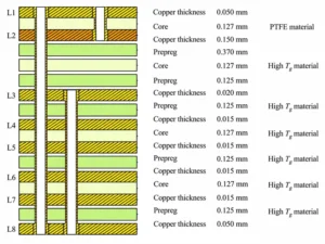
This board features an 8-layer design consisting of a hybrid laminate of PTFE high-frequency material and FR-4 high-glass transition temperature (Tg) material, where L1 and L2 are PTFE layers, and L3 and L8 are high-Tg layers.
The prepreg (PP) between L2 and L3 has a thickness of 0.612 mm. Before stack-up optimization, the stack-up did not include a copper-free substrate (Core), and the PP thickness was 0.488 mm; the PP thickness between all other layers was 0.125 mm.
Among the corresponding layers in the stack-up, only the copper on Layer L3 has a thickness of 20 μm, while the copper thickness on all other layers is 15 μm—a relatively small difference, as shown in Figure 1.
Furthermore, the copper residue rates for layers L1 through L8 range from 69% to 71%.
Engineering data analysis of layers L1, L3, L5, and L8 shows uniform circuit pattern distribution across these layers with no obvious localized gaps.
2. Determine the Manufacturing Process
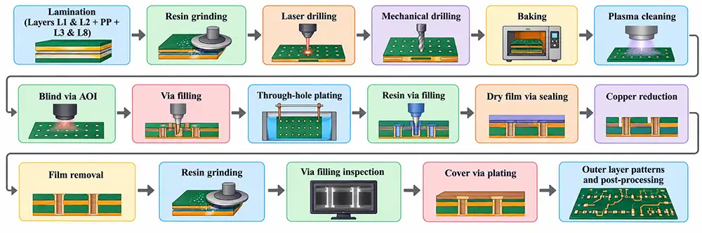
Layers L3 & L8: (L4 & L5 / L6 & L7) Sheet Cutting → Inner Layer Pattern → Inner Layer Automated Optical Inspection (AOI) → Laminating → Drilling Pilot Holes → Baking → Plasma Treatment → Electroplating → Resin Via Filling → Dry Film Via Sealing → Copper Reduction → Film Stripping → Resin Polishing → Secondary Outer Layer Traces → Secondary Outer Layer AOI. L1 & L2: Material cutting → Inner layer patterning → Inner layer AOI.
Layers L1 & L8: Lamination (Layers L1 & L2 + PP + L3 & L8) → Resin grinding → Laser drilling → Mechanical drilling → Baking → Plasma cleaning → Blind via AOI → Via filling → Through-hole plating → Resin via filling → Dry film via sealing → Copper reduction → Film removal → Resin grinding → Via filling inspection → Cover via plating → Outer layer patterns and post-processing.
3. Analysis of Defective Copper Surface Indentations
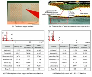
Further engineering verification confirms that visual defects primarily concentrate on the L1 surface, with numerous indentations appearing within a specific board area.
The defects discovered during final inspection matched the shape observed after lamination, as shown in Figure 2 (a).
Researchers conducted a cross-sectional analysis of the indented area corresponding to the conductor position in Figure 2(a), with the results presented in Figure 2(b).
The analysis verifies that PP debris pressing against the copper substrate of the L1 layer primarily causes these indentations, a defect categorized as copper surface indentation.
4. Summary
1) Structural Parameters and Material Stack-up of the Laminated Board
Board Warpage Analysis: As shown in Figure 1, the overall laminated board thickness is 1.5 mm.
Its key design features are as follows: the core materials for layers L1 and L2 are PTFE high-frequency materials, with a thickness of 0.19 mm;
The PP thickness between layers L2 and L3 is 0.49 mm, while the PP thickness between layers L6 and L7 is 0.15 mm;
The core materials and PP in the other layers are all high-Tg materials.
Engineering data review shows that the residual copper rate ranges from 69% to 71% across layers L1 to L8, ruling out the impact of excessive inter-layer residual copper rate variation.
2) Root Cause Identification of Laminated Board Warpage
Among all interlayer pairs, only the copper thickness difference of 1.27 μm between layers L3 and L6 exists, which exerts a negligible impact and can be excluded from potential causes.
Comprehensive investigation and analysis confirm that mixed lamination of dissimilar materials and asymmetric stack-up serve as the primary causes of board warpage.
Additionally, the difficulty in controlling the flatness during the secondary lamination process makes it impossible to meet quality requirements, regardless of parameter optimization.
3) Formation Mechanism of Copper Surface Indentation and Residual Copper Defects
Analysis of Copper Surface Indentations As shown in Figures 2(c) and (d), researchers conducted microscopic observation on the indentation defects and performed energy-dispersive spectrometer (EDS) analysis.
The results show that the material inside the indentations has the same composition as the prepreg (PP) between layers L2 and L3.
Based on this conclusion, a preliminary judgment can be drawn. PP debris sticks to the copper surface of the L1 layer in the pre-stacking stage.
These PP particles form tiny depressions on the copper surface after lamination.
A resin polishing process is implemented after lamination to eliminate surface contaminants.
However, polishing cannot clear the foreign substances trapped inside these indentations.
This situation hinders the subsequent etching process. It finally causes residual copper.
The defect impairs the appearance and reliability of the circuit board.
Improvement Measures and Validation Results
Board Warpage Mitigation
1. Improvement Measures
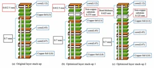
To optimize the process, we added PP and copper-free substrate layers of varying thicknesses between the L2 and L3 layers and employed different lamination methods, as shown in Figure 3.
Board warpage was assessed after standard lamination; the results are presented in Table 1 and Figure 4.
| Lamination Scheme | Lamination Process | Visual Inspection Result on Flat Surface | Warpage (%) |
|---|---|---|---|
| Scheme 1 (Original Stack-Up Lamination Method) | ① First lamination: Laminate L4&L5 + L6&L7 into L3&L8. ② Second lamination: Laminate L1&L2 + 2 PP sheets + L3&L8 into L1&L8. | Warpage at four corners | 2.21 |
| Scheme 2 (Optimized Stack-Up Lamination Method 1) | ① First lamination: Laminate L4&L5 + L6&L7 into L3&L8. ② Second lamination: Laminate L1&L2 + 1 PP sheet + copper-free substrate (0.375 mm) + 1 PP sheet + L3&L8 into L1&L8. | Diagonal warpage | 1.10 |
| Scheme 3 (Optimized Stack-Up Lamination Method 2) | ① First lamination: Separately laminate L1&L2 + 2 PP sheets + copper-free substrate, and L4&L5 + L6&L7 into L3&L8, forming two independent core boards. ② Second lamination: Laminate L1 + 2 PP sheets + copper-free substrate (0.125 mm) + 1 PP sheet + L3&L8 into L1&L |
Table 1. Different Stack-Up Lamination Schemes and Board Warpage Test Results
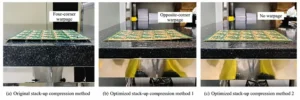
2. Test Results
In the first lamination stage of Option 3, technicians laminate two separate core boards: one consisting of L1 & L2, two PP sheets, and a 0.125 mm copper-free substrate, and another comprising L4 & L5 and L6 & L7 layers.
Then, one sheet of PP was inserted between the two core boards for a second lamination to form L1/L8. After lamination using this method, the board appeared visually flat.
It can be seen that adopting Approach 3 provides better control over board warpage and meets the customer’s specifications (board thickness of 1.58 mm, warpage <0.53%).
Improvements to Panel Surface Indentations
1. Improvement Plan
The primary cause of indentations on the copper surface of the L1 layer is PP debris adhering to the copper surface prior to lamination, a phenomenon related to the relatively soft nature of PTFE material.
How, then, can we prevent PP debris from adhering to the PTFE panels during the process from PP blanking to pre-stacking and lamination?
This study will implement control measures throughout the process from browning to the laminating press and verify the effectiveness of the improvements.
The specific steps are as follows.
(1) Browning:
Clean the work surface and rollers of the browning unloading machine section;
Conduct a 100% visual inspection of the core boards after browning; remove and isolate any damaged boards;
(2) Post-brown-coating Film Application:
Clean the surface of the brown-coated core sheets with a lint-removing roller before applying the film;
After film application, peel off the protective polyester film and apply the protective film flat against the inner molding area within the pin holes;
(3) PP Cutting and Edge Sealing:
Clean tools such as transport carts, and ensure the air outlet is vertically aligned with the PP edge while sweeping across it at a constant speed.
Dry all four edges in sequence, and visually confirm that the PP edges show a color change and are free of fiber residue;
(4) Film Removal/Cleaning Before Lamination:
Clean the work surface and surrounding area before lamination; after removing the protective film, inspect the panel surface.
If PP debris or other foreign objects are found, clean the surface immediately (use a wax cloth to clean the L1 surface first on the cart, then clean the L1 surface again on the lamination table;
Once cleaning is verified, directly cover with copper foil and other auxiliary materials);
(5) Positioning and Cleaning Before Lamination:
Clean the work surfaces of the hot-melt machine and riveting machine; during hot-melt bonding, place the layer with the protective film on top;
After riveting, use a PP spacer to separate the layers and place them individually on a dedicated pre-press cart;
(6) Pressing Process:
Inspect the panel surface; if PP debris or other foreign objects are found, clean the surface immediately;
Once cleaning is verified as satisfactory, directly cover the panel with copper foil and other auxiliary materials.
2. Validation Results
After implementing the above control measures, production inspectors confirmed that the process has essentially eliminated panel surface indentations.
The defect rate has dropped from the previous 100% to below 2.5%, returning to normal levels, which validates the effectiveness of the improvements.
The core of the aforementioned process controls lies primarily in ensuring thorough cleaning at each process step.
Operators attach targeted protective films to the brown-oxidized L1 and L2 PTFE substrates.
They perform a dedicated film removal and cleaning process before lamination.
This method thoroughly eliminates residual brown-treatment contaminants, PP debris, and foreign particles from both the prepreg and processing equipment.
It significantly improves the overall cleanliness of the board surface before lamination.
This demonstrates that the improvement plan is effective.
Factories can incorporate this lamination process control plan for the proposed stack-up design into standardized operating procedures, ensuring long-term stability of lamination quality.
Conclusion
In summary, millimeter-wave radar circuit boards designed with an asymmetric stack-up of PTFE and high-Tg materials experience severe warping and concavity on the secondary copper layer of the PTFE side during normal production.
This study developed and validated three solutions to address board warpage.
Comparative analysis of experimental results identifies the optimal solution.
The core strategy is to optimize the laminate stack-up structure and adopt a two-stage lamination process.
The first pressing operation bonds L1 and L2 with two pieces of PP and a 0.125 mm copper-free substrate.
Meanwhile, L4&L5 and L6&L7 are pressed together to form the L3 and L8 layers.
The second pressing operation assembles the copper-free L1 substrate with the prefabricated L3 and L8 layers to complete lamination.
This approach eliminates the overall stress caused by the asymmetric stack-up and meets the customer’s quality requirement of board warpage <0.53%.
Researchers identified the source of copper surface indentations through cross-section and EDS analysis.
Operators clean dust and debris from relevant equipment between the browning and pre-stacking stages.
They also clean the PP surface after cutting. Workers attach a protective film to the cleaned PTFE core board and peel off this film before pre-stacking.
Operating in this manner effectively removes PP debris and prevents it from adhering to the surface of the PTFE core board.
Batch validation confirms that manufacturers can significantly reduce the defect rate of copper surface indentations to a controllable range.
In subsequent production processes, engineers can continuously optimize control details to further lower the defect rate.

