
It is a common challenge for engineers to discover during the layout process that there are not enough layers to properly complete the design.
Designers should adopt systematic layout planning for complex circuit boards to avoid rework. This paper explores the core planning issues designers must resolve before starting routing.
How much physical board area do designers need for a valid layout (primarily determined by component and pin counts)?
How can engineers leverage schematics to guide component placement and eliminate pre-routing interference risks?
When should designers apply a ground tree structure rather than a ground plane?
There are several online tools available to help estimate PCB area and the number of signal layers required. Most of these tools require the following information:
What is the total number of components and pins?
What are the via pad ring width and drill hole sizes?
What is the minimum allowable trace width?
What are the functional voltage spacing requirements?
While these online tools are helpful, they are not comprehensive.
Most of them do not account for thermal considerations. They also ignore the current-carrying capacity of specific networks.
They fail to consider the increased voltage spacing required for functional or safety reasons.
Additionally, they neglect the additional design techniques and spacing needed to prevent crosstalk in highly sensitive circuits.
In short, these tools know nothing about real-world application scenarios.
This article will provide a set of guidelines to help you design better PCBs.
From Schematic to Layout
Schematic design always takes precedence; designers must thoroughly understand the contents of the schematic and the internal operating principles of the circuit.
Designers must attach paramount importance to this point.
As discussed above, component and pin quantities typically define the circuit board’s area and dimensions.
Meanwhile, the quantity and function of internal networks and transmission lines define the layer stackup.
Designers should clearly specify these constraints within the schematic (or design proposal), yet practical projects often fail to meet this requirement and occasionally face severely limited available space.
When placing components on the schematic, designers should reflect actual layout requirements, or at least add appropriate annotations to the schematic to assist with the layout.
Designers should label nodes requiring compact arrangement as “compact” on the schematic and group circuits that demand close physical placement next to each other on the schematic.
Practices such as these will facilitate the subsequent component placement process.
Some designs (such as RF or high-speed digital circuits) require attention to physical distances (propagation delay) or other analog characteristics (e.g., precision analog circuits);
Other designs treat circuit components as lumped elements and render physical distances non-critical.
Designers should appropriately annotate all the above details on the schematic to clarify key parameters for schematic-to-PCB design conversion.
Device Layout and Routing
To a certain extent, layout schemes can also influence schematic design.
This is necessary when mitigating design compromises brought by low-layer-count boards.
It also applies to the design of multi-board systems, including board-to-board connector arrangements.
The application of differential signaling is a typical example (Figure 1).
This technique is commonly used for analog or digital signals that require long-distance transmission, such as in cable transmission scenarios.
This technique transmits positive and negative signals simultaneously through a cable (excluding the ground line).
The displacement currents generated by each signal cancel each other out on the ground line.
This effect forms a communication path. The path is virtually immune to common-mode interference and electromagnetic interference (EMI).
The same technique can also be used for short-distance transmission on PCBs to maintain ground integrity;
It is suitable for precision or sensitive analog signals, or when PCB trace lengths are excessively long.
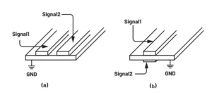
Figure 1a routes two equal-length complementary signal lines in parallel and shares a unified ground plane for them.
Figure 1b distributes signal lines across different layers and isolates them with ground planes.
Since the physical positions of the signals are nearly identical, the coupled interference signals should also be consistent.
Therefore, differential signaling can effectively suppress coupled noise.
Sometimes it is not possible to eliminate current in the ground lines;
Under such circumstances, designers must partition the ground plane into multiple regions or adopt a ground tree structure as an alternative.
Layout geometry determines whether engineers need to implement these approaches.
Designers may adjust the schematic to split ground lines for easier implementation:
Maintain the same network but use different ground line symbols (such as gnd1, gnd2, gnd3, etc.), thereby enforcing ground line separation in the layout.
Ground Trees and Ground Planes
Basic Electromagnetic Principle of Natural Energy Minimization and Ground Plane Characteristics
Nature always tends to minimize the energy required at the source (whether for storage or dissipation).
For AC signals in traces above a ground plane, the signal ground return current always flows along the ground plane directly beneath the signal trace.
While Faraday’s law alone would suffice to confine the electromagnetic field, a complete ground plane is still provided around the signal traces (stripline designs have two ground planes).
A solid ground plane offers superior high-frequency decoupling performance.
It serves as a lower-impedance power source at higher frequencies.
Large-area copper foil achieves better confinement of both DC and AC electromagnetic fields.
Given this, why use a ground tree structure instead of a ground plane?
Figures 2 and 3 illustrate these two methods, along with formulas describing the impedance of lossy transmission lines.

Let’s first look at this formula: under DC conditions (ω = 0), the line impedance is √((R/G)) (i.e., the loss component).
For the current return path, 1/G also represents resistance; therefore, the current flows back along the path of least resistance, making full use of all available copper foil.
This phenomenon is essentially nature’s way of minimizing energy. At these low frequencies, the energy consumed by I²R losses far exceeds the energy stored in the ground loop’s inductance.
When ω = 0, the DC return current is no longer confined to the area directly beneath the signal trace, and the current flow in the copper foil creates a voltage drop across the ground plane.
Layout Principle and Implementation of Ground Tree Structure
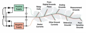
When constructing a ground tree, start with the transformer and prioritize routing the currents with the highest noise levels back to ground (Figure 2).
Next, continue to route other ground return currents into branches that terminate at the ground point.
This method converts ground noise and errors into common-mode signals that are easier to suppress.
Note: Some branches may be longer to accommodate component placement.
Finally, ground copper foil can be laid across all branches to reduce power supply impedance without compromising the effectiveness of this method.
Comparative Analysis of Ground Plane Layout and Frequency-Domain Characteristics
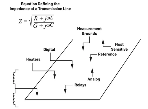
First, designate both sides of the ground plane as dedicated return paths for adjacent signal layers.
If a ground tree structure is not used, whether ground current noise sources at low frequencies result in common-mode errors or differential-mode errors will depend entirely on component layout.
At high frequencies, inductance limits the total current amplitude; therefore, reducing energy storage becomes a key parameter for minimizing energy extraction at the source.
At low frequencies, the above-mentioned currents will produce ground voltage drop.
This voltage drop may result in measurement errors. The actual impact depends on component placement.
It is also related to the position of the ground reference point for key measurements.
Consequently, the potential at the ground point is not zero everywhere.
Next, we analyze the ground plane layout shown in Figure 3.
This method ensures that high currents do not produce detectable voltage drops by controlling the return current paths.
In the schematic, each branch can be labeled distinctly to reinforce the architectural design of the PCB.
In practice, using a ground tree significantly increases the layout workload, as controlled (and narrow) field spaces must still be provided for all transmission lines to limit AC electromagnetic fields.
All ground copper foil fills shown in Figure 2 are necessary to address this issue.
Conclusion
Decisions made before routing determine the success or failure of the subsequent design.
By adapting the schematic to meet layout requirements and selecting an appropriate grounding architecture early on, you can lay a solid foundation for the circuit board to operate as intended.
Whether the design employs a solid ground plane or a precisely controlled ground tree, the goal remains the same:
To limit electromagnetic fields, control return currents, and prevent noise from coupling to sensitive nodes.

