
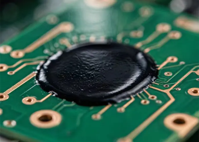
PCB Inks in Modern Electronics Manufacturing: Types, Functions, and Selection Principles
Printed circuit board (PCB) ink is an indispensable key material […]
Printed circuit board (PCB) ink is an indispensable key material […]
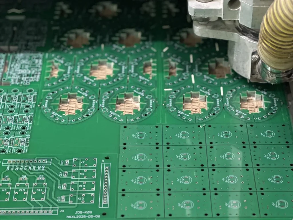
In the field of high-end printed circuit board (PCB) manufacturing, milled vias (such as dogbone vias and small square vias) serve as core microstructures for interlayer interconnection and precise signal transmission.
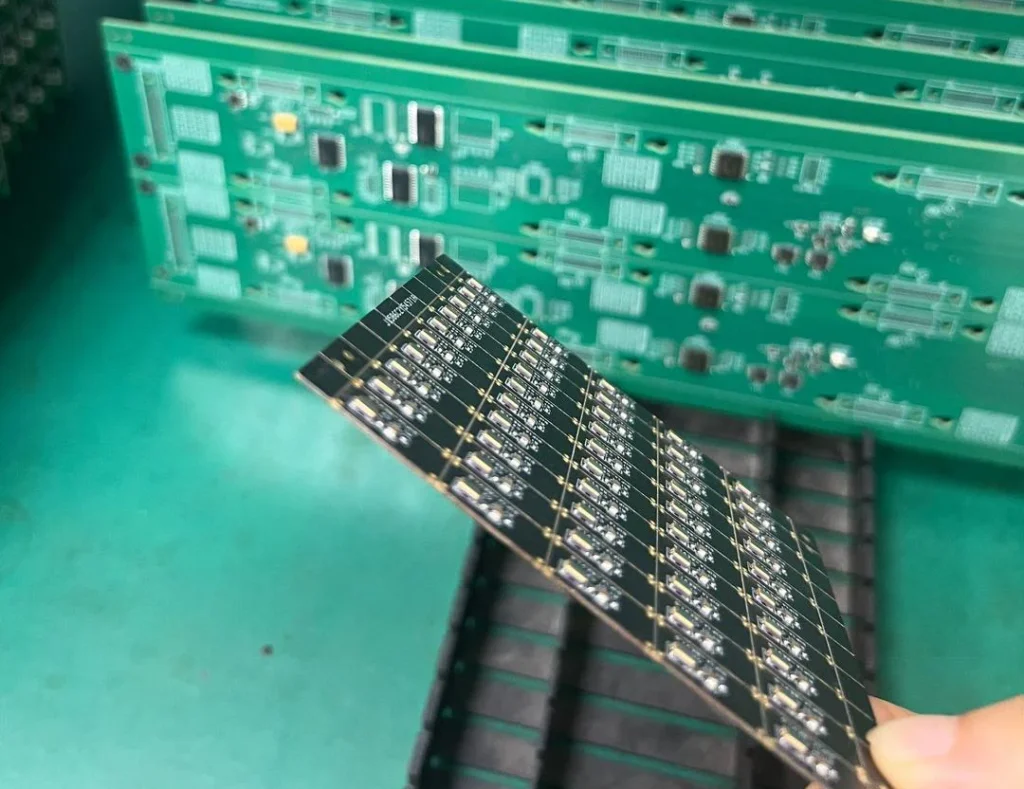
Some printed circuit boards (PCBs) require the large copper surfaces to be coated with gold, a process known as “gold plating.”
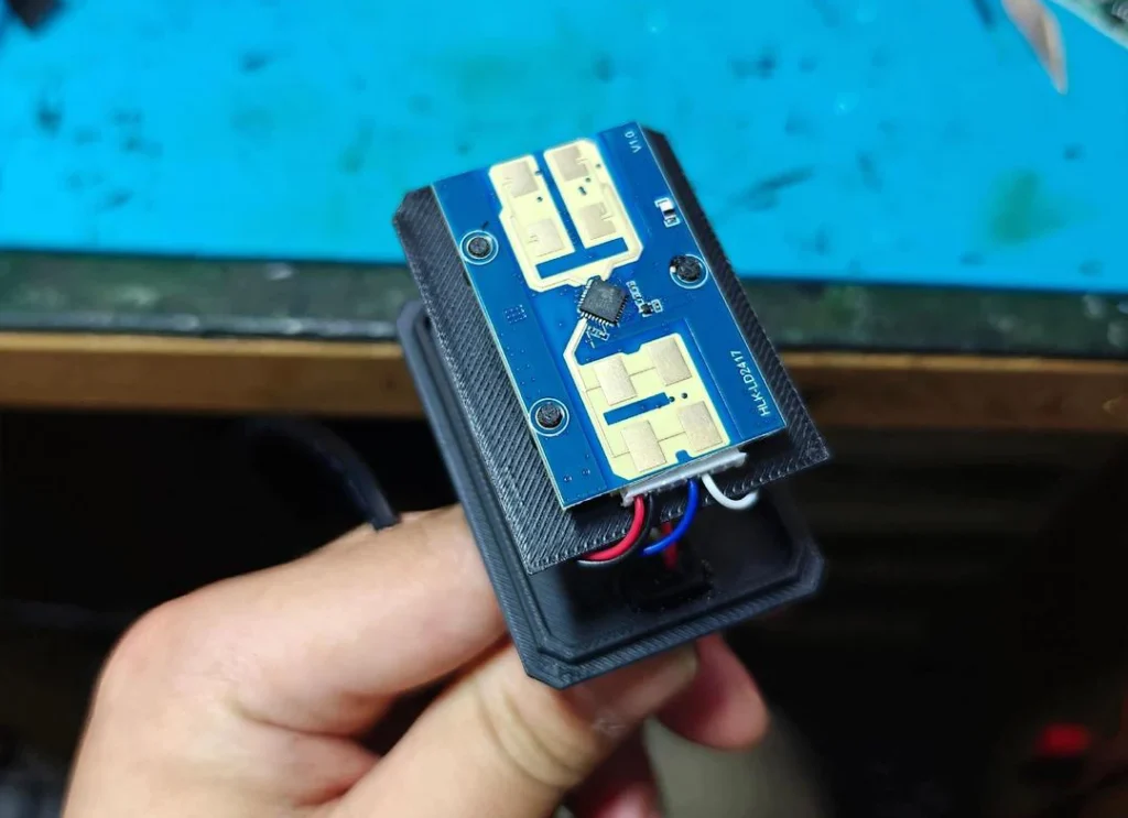
As millimeter-wave radar technology finds increasingly widespread application in fields such as autonomous driving, aerospace, and security surveillance, the demand for high-performance printed circuit boards (PCBs) has grown accordingly.
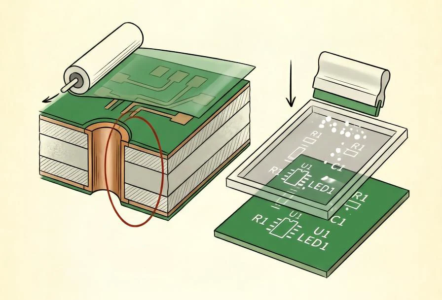
Solder mask application is a core process in PCB manufacturing that determines yield and reliability, and pre-treatment is the cornerstone of its success.
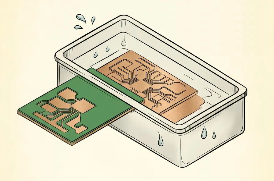
The primary purpose of pretreatment in each PCB manufacturing process is to achieve two key objectives: cleaning and surface roughening.
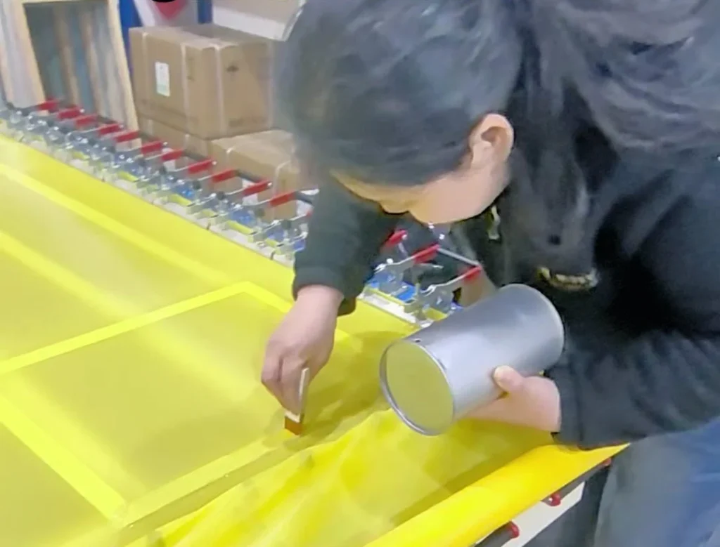
PCB silkscreen is a critical layer in printed circuit board (PCB) design that provides essential information for assembly, testing, and troubleshooting.
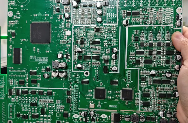
Printed circuit boards (PCBs) provide interconnections for electronic components and parts, forming modules or finished products with specific functions.
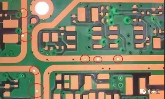
Via holes serve to interconnect circuit traces. The advancement of the electronics industry has driven the development of PCBs while imposing higher demands on printed circuit board manufacturing processes and surface mount technology.
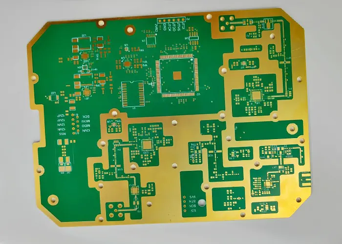
As the functionalization of multilayer printed circuit boards (PCBs) continues to advance, multilayer PCBs are often designed with stepped structures featuring varying board thicknesses.