
In recent years, aviation equipment has been evolving toward greater intelligence and integration, placing higher demands on the functionality and performance of onboard electronic aviation products.
Consequently, the complexity of circuit designs for these products has gradually increased, circuit structures have become more intricate, and the defect rate in printed circuit board manufacturing has risen.
Impact of PCB Failures in Aviation Systems
Failures in aviation products can directly endanger pilots and lead to the failure of flight missions.
When a circuit board is returned to the factory for repair due to defects or failure, maintenance and testing personnel often find it difficult to immediately pinpoint the fault.
This can result in significant time spent troubleshooting individual components, thereby delaying the repair process. Common types of PCB faults include open circuits, short circuits, glitches, and missing traces.
The adoption of intelligent solutions for efficient PCB defect detection is of great significance for reducing product defect rates and improving the quality of aerospace products.
Limitations of Traditional and Existing Detection Methods
Traditional manual PCB defect inspection methods require significant manpower and are highly susceptible to human subjectivity, making it difficult to ensure consistent inspection efficiency.
In machine vision, the RetinaNet visual recognition solution can identify PCB defects, but it suffers from limited accuracy in detecting smaller defects.
The YOLOv5-based PCB surface defect detection solution achieves a balance between speed and accuracy, but it does not support deployment on embedded devices.
Compared to YOLOv5, the YOLOv7 model offers greater data flexibility, optimized network performance, and improved computational efficiency; therefore, YOLOv7 was selected as the basis for training the PCB defect detection model.
To enable edge deployment, the Fudan Microelectronics FMQL100TAI heterogeneous hardware platform was selected after a comprehensive evaluation of factors including cost, power consumption, and architecture.
The FMQL100TAI chip features CPU, NPU, and FPGA functional modules, supports the edge deployment of neural networks, and provides a complete, compatible development environment.
Model Development and Training
YOLOv7-tiny Model
YOLOv7-tiny is a lightweight version of YOLOv7 designed to significantly reduce computational load and model parameters while maintaining high detection accuracy, making it suitable for resource-constrained edge devices.
It retains YOLOv7’s cascade-based model scaling strategy and improves upon the Efficient Long-Range Aggregation Network (ELAN).
With fewer parameters and faster detection speeds while ensuring detection accuracy remains largely unchanged, it is better suited for real-time defect detection on PCBs.
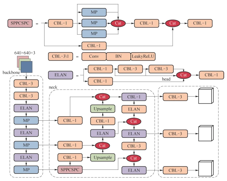
Figure 1 shows the network architecture of YOLOv7-tiny. The overall structure consists of three main components: the backbone network, the feature pyramid, and the detection head.
Fixed-size images are fed into the backbone network for feature extraction. Next, the extracted feature maps are fed into an SPPCSPC module—an optimized version of the SPP architecture—for processing.
Afterward, the system sends them to the feature fusion layer and employs an aggregated feature pyramid structure to enhance the entire pyramid of feature maps.
This process propagates saliency information from lower layers to upper layers, preserving richer feature details, while simultaneously feeding the fused features back down to enhance detection details.
Finally, the detection head receives these semantically rich feature maps and uses convolutions to predict feature maps at different scales.
The system applies anchor boxes to the target feature maps and generates a final output vector containing class probabilities and target boxes, thereby enhancing the network’s robustness for defect detection at various scales.
Model Training
The dataset used is the open-source DeepPCB dataset, which contains over 1,500 image pairs covering six of the most common printed circuit board defects: open, short, mousebite, spur, pinholes, as well as common PCB defects such as spurious and copper.
The DeepPCB dataset uses absolute coordinates of the top-left and bottom-right corners to annotate detection targets.
To adapt it to the YOLOv7-tiny model, the system converts the dataset into the COCO format, namely [type, (x₁, y₁), w, h].
In this format, type represents the defect category ID value for various defect patterns.
(x₁, y₁) indicate the relative coordinates of the center point of the manually annotated bounding box.
w and h represent the relative width and height of the bounding box with respect to the original image.
The dataset contains a total of 1,500 processed images, and the researchers divide them into training, validation, and test sets in a 3:1:1 ratio, with 900, 300, and 300 images, respectively.
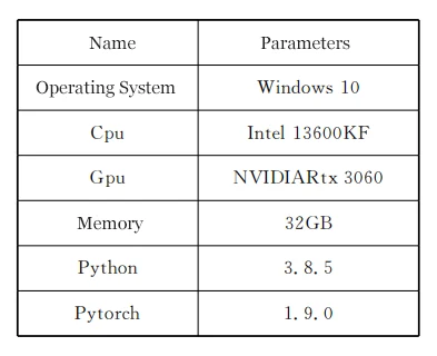
Table 1 presents the hardware and software environment for model training.
The input image size is 640 × 640. Stochastic Gradient Descent (SGD) updates the learning rate, and a weight decay value of 0.00005 is set.
The training runs for a total of 300 epochs, with each batch containing 32 images.
Hardware Deployment
Once training is complete, deploy the model to a hardware platform powered by the FMQL100TAI chip as the main processor to complete the edge deployment.
Introduction to the FMQL100TAI Chip
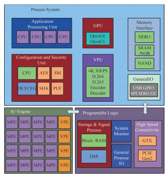
The Fudan Micro FMQL100TAI chip features a multi-core bus-interconnected architecture and includes AIE (NPU), PL (FPGA), and PS (CPU) modules. Figure 2 shows the chip’s architectural diagram.
The PS module includes a quad-core A53 GPU that supports OpenCL and OpenGL, and supports 4K/30fps video encoding and decoding.
The AIE module supports INT8 (27.5 TOPS) or INT16 (27.5/4 TOPS) compute, and also multi-level caching to enhance internal bandwidth.
Compared to the previous-generation 45TAI chip, the FMQL100TAI moves the NPU (AIE) unit from inside the PL to a separate module outside the PL, which facilitates internal chip routing and reduces signal transmission latency.
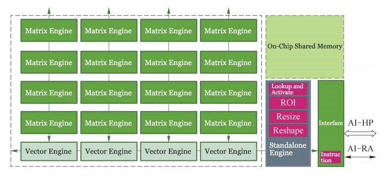
Compared to FPGA hardware acceleration platforms, the FMQL100TAI features a programmable PL section and an AIE neural network computing unit, as shown in Figure 3.
The AIE accelerates the computation speed of convolutional neural networks, while the PL section reduces algorithm preprocessing and postprocessing times and enables the construction of hardware operators.
Compared to the VERSA series chips from Xilinx, the FMQL100TAI’s AIE module adopts an asymmetric architecture, which facilitates users’ access to matrix operation resources and interface modifications.
Model Compilation and Deployment Process
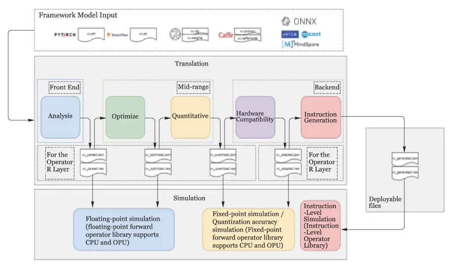
After determining the hardware platform, Fudan Micro’s ICRAFT 3.6.2 compilation tool completed the analysis, optimization, and quantification processes for the aircraft printed circuit board defect detection algorithm model on a Windows system.
The . .pt files generated during the Python training process into .json and .raw files, so that the FMQL100TAI chip can call the model interface, as shown in Figure 4.
Before compilation, configure the model image input format in the script configuration file .toml, and set the output paths for the intermediate files generated during the compilation process—.parsed, .optimized, and .quantized—to the same folder.
After modifying the configuration file, enter the `compile` command to complete the compilation, generating the `BY.jason` and `BY.ram` files.
To verify that the ICRAFT-compiled model matches the pre-training model, users must perform verification in a Windows environment.
Select a test image at random, compare the test results, and determine whether the results match those obtained before compilation.
Application Development and System Deployment
Once you have confirmed that the ICRAFT model has compiled successfully, you can begin developing the top-level application in the VMVARE Linux environment.
In the top-level program’s .cpp file, you need to call the pre-compiled model to perform the YOLOv7-tiny neural network computations.
The top-level program must also read data and apply non-maximum suppression to the model’s output to enable bounding box display.
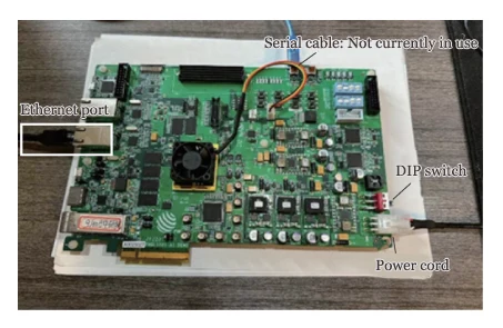
After writing and compiling the application in the Linux environment of the host computer’s virtual machine, power on the FMQL100TAI development board, connect the Ethernet cable (as shown in Figure 5), and set the host computer’s IP address to be within the same subnet.
Using the Mobaxterm network communication software, you can view and control the embedded Linux system on the development board.
Transfer the application and AI models to the 100TAI development board via the network interface. This completes the hardware deployment.
Test Results
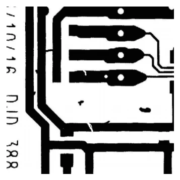
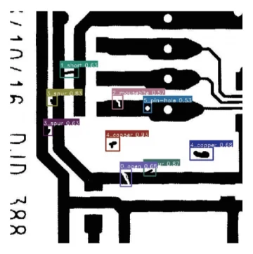
The test results show that the PCB defect-detection solution deployed on the terminal can fully identify even minor PCB defects.
According to the printout information from Mobaxterm, the image input latency during single-image inference was 3.74 ms, and the latency for reading the inference results
was 1.16 ms, and the hardware acceleration duration was only 8.74 ms.
Conclusion
The experiments demonstrated that:
① The YOLOv7-tiny model is capable of detecting detailed defects and faults in printed circuit boards.
② The 100-TAI hardware environment provides sufficient computational resources, making it well-suited for the YOLOv7-tiny model and delivering good inference speeds.

