
The use of Automated Optical Inspection (AOI) equipment to verify the correct assembly of product components has become a widespread practice.
In the field of integrated circuits, AOI primarily inspects components soldered using Surface Mount Technology (SMT) and components bonded in micro-assembly processes.
With the continuous evolution of AOI technology, its scope of inspection has expanded to include quality control aspects, such as detecting component assembly misalignment and solder joint defects.
The AOI testing logic involves inspecting products according to a predefined program.
If product characteristics satisfy the program requirements, the system generates a “Pass” record to indicate that the product passes the AOI test and requires no manual verification.
If product characteristics fail to meet the program requirements, the system generates a corresponding “Not Good” (NG) record to indicate that the product fails the AOI test.
Operators must then verify each NG record manually and perform supplementary manual microscopic inspection when needed to confirm whether the product contains a real defect.
Users can categorize NG records as true defect records or false positive records according to their correspondence with actual defects.
AOI may classify items that meet the program’s pass criteria as failing, thereby generating false positive NG records.
The primary causes of false positives stem from the AOI system’s image comparison logic and algorithms.
When AOI generates more false‑positive NG records, manual verification workload rises.
Inspectors become more likely to overlook real product defects, which ultimately causes missed defects and shipment of defective products.
Therefore, reducing false-positive NG records is a critical task for improving the effectiveness of AOI testing.
Statistics show that during AOI testing of integrated circuit products, there are a large number of false “NG” detections in areas such as mark recognition, detection frame misalignment in panelized products, solder joint defects, and polarity errors in bare chips.
This paper analyzes and proposes improvements for these four types of false “NG” detections.
Analysis of NG Misclassification Phenomena and Improvement Measures
Mark Recognition NG Misclassification
1. Mark Recognition Defect Phenomena
Mark recognition typically employs a template-matching algorithm.
When the difference between the recognized mark pattern and the reference pattern defined in the AOI program exceeds the allowable range, the system generates a defect record.
For AOI programs targeting module and component circuit products, engineers typically select the mark from mark patterns designed on the printed circuit board (PCB).
When the surface of the mark pattern on the PCB is made of tin, false NG detections are likely to occur.
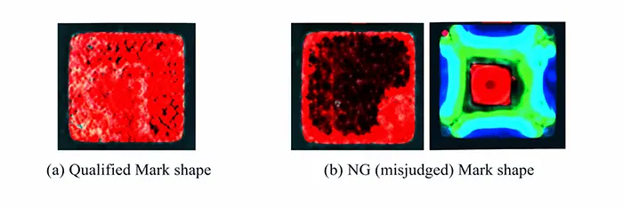
The imaging of tin-based marks in AOI is shown in Figure 1.
Increasing the number of mark templates or widening the allowable tolerance for mark patterns (which may lead to misidentification) cannot completely resolve the issue of false negative results.
2. Analysis of Mark Recognition Failures
As shown in Figure 1, the differences between acceptable and misidentified Marks primarily lie in their color and brightness.
Acceptable Marks typically exhibit a uniform bright red color, whereas misidentified Marks display variations in brightness, appearing as red, black, or combinations of red, black, green, and blue.
Physical comparisons confirm that the differences in color and brightness are primarily due to varying degrees of “bulging” in the Mark.
This “bulging” results from inherent defects in the Mark’s design or from solder adhesion.
When the Mark’s “bulging” is minor, it exhibits red and black features with varying brightness, as shown in Figure 2.
When the “bulging” is severe, the Mark exhibits red, black, green, and blue features with varying brightness, as shown in Figure 3.
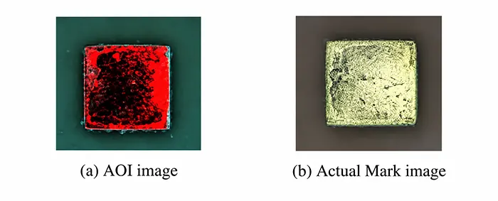
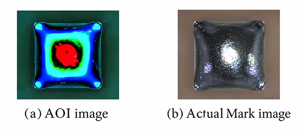
The color and brightness characteristics of the Mark displayed on the tin material follow the same principle as the varying brightness of red, green, and blue colors formed by solder wicking on components.
However, the black area at the junction of the red and green Mark patterns in Figure 3 contradicts the color theory that mixing red and green produces yellow.
This shows that, at the junction of red and green, light reflects into an area outside the camera’s field of view.
According to the principle of specular reflection, when the angle of incidence of the AOI device’s light source does not match the height of the camera receiving the reflected light, the reflected light cannot return to the camera.
This causes both minor and severe “balling” issues to result in a black feature at the boundary between the red and green areas of the Mark graphic.
3. Measures to Reduce False Rejects in Mark Recognition
Method 1: Adjust the light source angle. AOI equipment manufacturers shall optimize the matching between the incident angle of the light source and the camera installation height, so that the camera properly captures light reflected from the mark surface.
This method applies to the design, R&D, and installation stages of AOI equipment.
Operators cannot adjust the light source angle on in-service equipment during operation.
Method 2: Change the light source color by applying different light sources during mark recognition.
This method is suitable for situations where the mark pattern has uniform brightness.
As shown in Figure 1, the mark patterns that cause false NG detections exhibit uneven brightness due to their own morphology and issues with the light source angle of the AOI equipment; changing the light source color cannot reduce false NG detections.
Method 3: Modify the recognition algorithm and use a color-based algorithm to extract features from the mark patterns that result in false NG detections.
This method is suitable when there are no similar patterns surrounding the mark that match its color and brightness characteristics;
However, as PCB products become increasingly smaller and more precise, product structures can no longer meet this constraint.
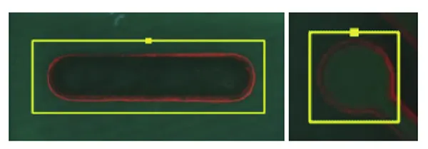
Method 4: Modify the recognition pattern by selecting other patterns on the PCB as the mark, as shown in Figure 4.
This method is suitable for situations where the appearance of PCB patterns is consistent and stable.
When choosing this method for improvement, the mark pattern is easy to select and offers versatility.
Misalignment of Inspection Frames for Panel Assembly Products: False “NG” Calls
Panel assembly refers to the process of combining a certain number of products from the same batch into a single fixture during assembly.
1. Detection Frame Misalignment NG Phenomenon
False positives of detection frame misalignment NG relate to the mark configuration method that AOI equipment manufacturers define.
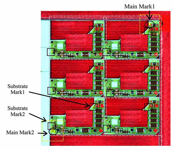
When users adopt a configuration with one set of master marks (which must sit on two different panels at diagonal positions of the whole panel assembly) and multiple sets of panel marks matching the panel count, as illustrated in Figure 5, the AOI system tends to produce false NG judgments.
When the AOI program runs, it first identifies the main marks and calculates the deviation between their actual positions and the set positions, which is the offset detected for the main marks.
It then locates the inspection frames for each panel.
The system identifies panel marks together with these inspection frames and calculates the deviation between their actual positions and preset positions; this value represents the detected offset of the panel marks.
In Figure 5, the elliptical box represents the main mark, and the square box represents the panel mark.
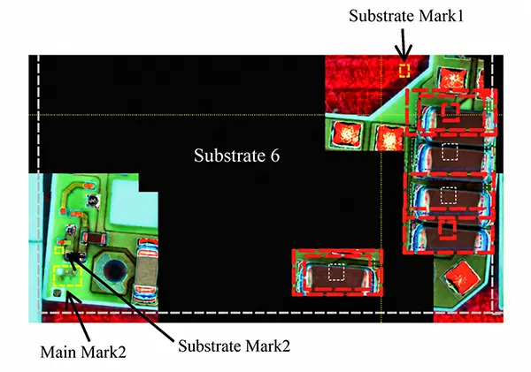
When panel 6, which has main mark 2, is placed at an angle or is misaligned, a false positive for capacitive detection box misalignment occurs, as shown in Figure 6.
False NG judgments may appear during the inspection process.
Common countermeasures include repositioning the panel assembly and setting more precise positioning limits for it.
Another option is to increase the allowable deviation of the detection frame, yet this risks overlooking real defects.
Alternatively, expanding the recognition range of the detection frame may trigger false positives by capturing positions of other components.
None of these conventional methods can thoroughly eliminate false NG detection problems.
2. Analysis of False “NG” Detections Due to Detection Frame Misalignment
The operating logic of the Mark needs to be confirmed. The offset value detected by the main Mark is adopted to correct its own position.
It also adjusts the actual positions of the detection box and the panel Mark on the corresponding panel.
In contrast, the offset value detected by the panel Mark is used for self-position correction.
It further adjusts the actual position of the detection box on the panel where it resides.
When both a Master Mark and a Panel Mark are present on the same panel, the program will prioritize the offset value detected by the Master Mark and will not use the offset value detected by the Panel Mark.
This leads to the following scenario. Panel 6 is equipped with main Mark 2.
If Panel 6 tilts or becomes misaligned, main Mark 2 supplies the offset value for calculation.
This offset value corrects the position of main Mark 2 itself. It also adjusts the positions of all detection boxes and panel marks on Panel 6.
At this point, the capacitor detection box has already deviated from its actual position.
During the inspection of panel 6, the program does not readjust the detection frame positions but proceeds directly with the inspection.
Because the detection frames deviate too far from the actual positions of the capacitors—exceeding the range set by the program—this results in a false “NG” (non-conforming) judgment due to the offset.
3. Measures to Reduce False Positive Defect Calls Due to Misalignment
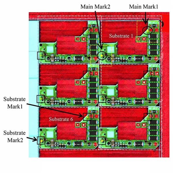
Adjust the mark settings to match the operating logic: place the main marks on one panel, and the panel marks on the other panels.
In other words, each panel can contain only one set of main marks or one set of panel marks, as shown in Figure 7.
In Figure 7, the oval boxes represent main marks, and the square boxes represent panel marks.
Main marks 1 and 2 are set on panel 1, while other panels, such as panel 6, are set with panel marks 1 and 2.
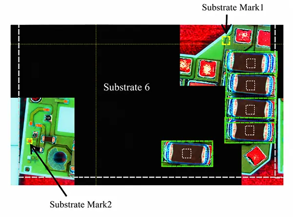
When panel 6 is placed at an angle or is misaligned, panels Mark1 and Mark2 use the detected offset to correct their own positions and adjust the positions of all capacitor detection frames, ensuring that the detection frames align with the actual positions of the capacitors.
The detection frames pass the misalignment check, as shown in Figure 8.
False Positive Calls for Defective Solder Joints
1. Phenomena of False Positive Calls for Defective Solder Joints
Defective solder joint detection is a common method used to inspect solder joint quality, conducted in conjunction with SMT component placement accuracy checks and supplemented by manual visual inspection.
It typically includes three inspection items—cold solder joints, insufficient solder, and exposed copper.
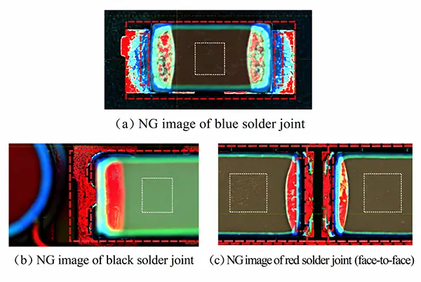
An example of a false “NG” determination for a qualified solder joint is shown in Figure 9.
The light source angle of AOI equipment is non-adjustable during operation.
Changing the light source color may cause missed solder joint defects.
Therefore, modifying the parameters of the solder joint detection box is a commonly adopted method. This approach is used to reduce false negative detections.
However, adjusting these parameters is labor-intensive, and it is impossible to fine-tune the parameters in a single debugging session to accommodate all product models, making it difficult to effectively reduce false negative detections.
2. Analysis of False Rejections for Defective Solder Joints
An analysis of false rejection phenomena reveals that there are two main causes for false rejections of defective solder joints.
First, when product types change, both pass and fail solder joints exhibit various new characteristics.
The original inspection parameters are unable to cover these characteristics, leading to false NG detections.
For example, in addition to exhibiting the dark blue characteristic set as “pass” in the program, acceptable solder joints may also display characteristics such as light blue, dark blue-green, and light blue-green, as shown in Figure 9(a);
Non-conforming solder joints—that is, pads with no solder or insufficient solder—may exhibit characteristics such as yellow in addition to the red and white characteristics defined as non-conforming by the program.
Second, as product assembly density increases, the characteristics of pass solder joints may not match the dark blue characteristics set in the program, leading to false NG judgments.
The solder joint of a tall component may be next to the body of another tall component.
In such cases, red, green and blue light cannot reach the solder joint surface.
Or the reflected light fails to return to the camera. Consequently, qualified solder joints present black features in the image, as illustrated in Figure 9(b).
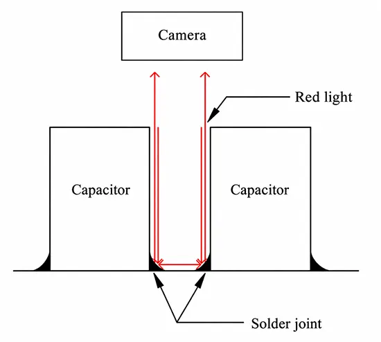
Two high-component devices of the same model may be arranged in a face-to-face configuration.
Under this layout, green and blue light cannot illuminate the solder joint surface. Or the reflected light cannot return to the camera.
In contrast, red light can be reflected by the solder joint surfaces of both components. This phenomenon is demonstrated in Figure 10.
This causes the pass solder joint to appear as a red “low-solder” feature, as shown in Figure 9(c).
3. Measures to Reduce False Positive Defects in Solder Joint Inspection
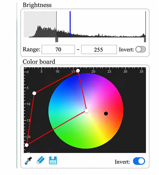
Using set theory, consolidate and optimize the solder joint inspection criteria to focus on a single criterion—insufficient solder (or an equivalent term)— and inspect only non-conforming solder joint characteristics.
Specifically, a solder joint is deemed non-conforming when it exhibits high-brightness color characteristics other than those of conforming solder joints (such as dark blue, light blue, dark blue-green, light blue-green, and black).
An example of the optimized solder joint inspection parameter settings is shown in Figure 11.
We consolidated and optimized the inspection items per solder joint for components, merging three items — cold solder joints, insufficient solder, and exposed copper — into one single item: insufficient solder.
This reduces inspection items per solder joint by two.
Using the inspection parameters shown in Figure 11, we built a new solder-joint database for the existing components on the equipment.
These parameters cover a wide range of characteristics of non-conforming solder joints and are highly versatile;
For newly deployed equipment or new component models, the “insufficient solder” inspection item integrates three pre-improvement inspection items: cold solder joints, insufficient solder, and exposed copper.
A single test can detect all three defects. This greatly reduces the workload of building AOI inspection libraries for new equipment or new component models.
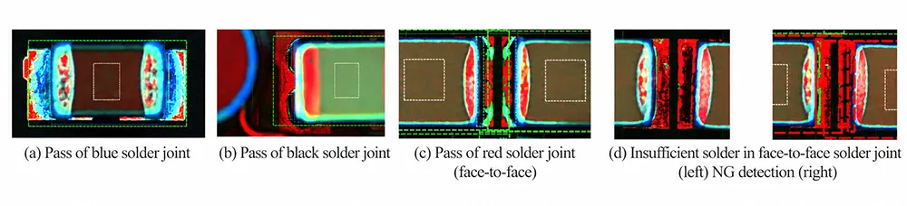
Figure 12 shows an example of solder joint inspection results after optimizing the inspection parameters.
False “NG” Calls Due to Polarity Errors in Bare Chips
1. Symptoms of False “NG” Calls Due to Polarity Errors
Bare chips are commonly used components in mixed-signal integrated circuit products.
For bare chips with polarity, it is necessary to detect assembly polarity errors.
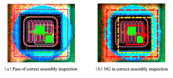
Image recognition algorithms are typically used for polarity detection; an example of a false NG call is shown in Figure 13.
A common approach is to add more reference images of the bare chips;
However, increasing the number of reference images may lead to missed detections of actual polarity errors, and thus fails to completely resolve the issue of false NG detections
2. Analysis of False Rejects for Polarity Errors
Bare-chip polarity-error false rejects mainly relate to the geometric features of the chip.
When a bare chip’s surface exhibits relatively uniform color or morphology, image recognition algorithms struggle to extract its polarity features.
In such cases, we raise the pass threshold to ensure the system detects all polarity errors.
However, raising the threshold reduces the allowable variation in chip images, and even subtle differences can result in false NG detections.
3. Measures to Reduce False Positive “NG” Calls Due to Polarity Errors
We use a color‑based algorithm to inspect the unique positions or shapes of pads on bare chips.
Since the color characteristics of pad patterns are stable, this approach effectively mitigates false “NG” detections caused by polarity errors resulting from subtle variations in the chips.
An example of the inspection results is shown in Figure 14.
Effectiveness of Reducing False-Negative Results
1. Overall False-Negative Rate Comparison Before and After Optimization
Before researching reducing false-negative results in AOI testing, the combined false-negative rate caused by the four issues mentioned above was 30.21%.
After implementing the improvement measures, we performed a three‑month statistical analysis of the false rejection rate in AOI testing and reduced the overall false rejection rate to 5.237%.
The specific data are shown in Table 1.
| NG Item | Inspection Points | NG Count | False-Positive Rate |
|---|---|---|---|
| Mark Recognition | 51,084 | 55 | 0.107% |
| Inspection Frame Misalignment | 23,006 | 16 | 0.069% |
| False Solder Joint | 113,144 | 3,790 | 3.350% |
| Polarity Error | 103,623 | 11,371 | 10.973% |
| Total | 290,857 | 15,232 | 5.237% |
Table 1. AOI Test NG False-Positive Rate Statistics Over Three Months
The table shows that bare die polarity errors yield a higher false positive rate than other false positives.
This mainly occurs because the parameter settings for extracting bare die polarity features via the color algorithm adopt a narrow range — a broader range may cause missed defects — so these settings cannot fully capture die features.
2. Multi-Condition Retest Verification of Optimization Effectiveness
Retests were carried out on the inspection points listed in Table 1 to verify the effectiveness of the improved measures.
We conducted the retests under multiple conditions.
These conditions included AOI tests with pre-improvement parameters and tests on downstream automated assembly equipment during product assembly.
We retested a total of 119,829 inspection points. After the improvement, we recorded zero missed defects, yielding a 0% missed defect rate.
When operators adopted manual visual inspection for rechecking 136,716 inspection points, they found 23 missed defects after the improvement, which produces a 0.017% missed defect rate.
The specific data are shown in Table 2.
| NG Item | Equipment Re-inspection Points (Detected / Missed / Miss Rate) | Manual Re-inspection Points (Detected / Missed / Miss Rate) |
|---|---|---|
| Mark Recognition | 1,726 (0 / 0) | 10,232 (0 / 0) |
| Inspection Frame Misalignment | 8,102 (0 / 0) | 12,308 (0 / 0) |
| Poor Solder Joint | 6,378 (0 / 0) | 113,144 (23 / 0.020%) |
| Polarity Error | 103,623 (0 / 0) | 1,032 (0 / 0) |
| Total | 119,829 (0 / 0) | 136,716 (23 / 0.017%) |
Table 2. Statistics on Effectiveness After Improvement
3. Analysis of Residual Missed Defects and Comprehensive Improvement Conclusion
The item missed after the improvement, as identified by manual re-inspection, was a defective solder joint.
The cause was abnormal characteristics present in localized areas of the solder joints, which were not clearly visible in the images.
When we retest with the AOI using pre‑improvement settings, the equipment also fails to detect these defects.
This shows the improvements did not cause the missed defects, and operators can eliminate such defects through manual microscopic inspection.
In summary, the improvements eliminated missed defects, significantly lowered the false negative rate, and markedly boosted inspection effectiveness.
Conclusion
This study analyzes the root causes of false NG detections.
These causes include mark recognition errors, panel detection frame misalignment, solder joint anomalies, and polarity misjudgment of bare chips.
We accordingly propose targeted improvement measures.
The strategies involve optimized mark pattern selection, standardized panel mark settings aligned with operational logic, integrated and refined solder joint inspection algorithms, and polarity detection algorithms adapted to chip structural characteristics.
These measures were then implemented in the AOI testing of integrated circuit products.
The test results demonstrate the effect of the proposed improvements. The false rejection rates of the four aforementioned defect types drop substantially.
This greatly improves the overall performance of AOI inspection and drastically cuts the manual workload required to verify false NG detections.
Consequently, inspectors can devote more attention to “NG” reports, enabling more effective detection and removal of genuine defects.
Following these improvements, there are still shortcomings regarding the detection of localized solder joint anomalies and the reduction of false positives for bare chip polarity errors; therefore, continued research in these areas is necessary.

