
Currently, mobile communications, high-performance computing (HPC), and artificial intelligence (AI) have become the mainstream of the electronic information industry, with semiconductor chips serving as the “brain” and “heart” of these electronic devices.
However, packaging substrates alone can realize chip functionality, and advanced packaging shapes the core technology that determines industrial competitiveness and the industry landscape.
Printed circuit boards (PCBs) serve as the carriers for chips and the foundation of electronic packaging.
The electronics circuit industry must keep pace with advancements in advanced packaging and gain a thorough understanding of it in order to make a meaningful impact.
Background of Advanced Packaging
The Slowdown of Moore’s Law and the Rise of Advanced Packaging
Semiconductor devices have always been the cornerstone of electronic equipment;
Upgrades to computers, mobile phones, and various electronic control systems are primarily driven by improvements in the functionality of semiconductor chips.
Over the past several decades, researchers have generally measured the development of integrated circuit (IC) technology based on Moore’s Law.
This law states that the number of transistors on an integrated circuit doubles every 18 to 24 months, bringing doubled device performance and halved production costs.
In recent years, Moore’s Law has faced challenges posed by physical limits and rising costs.
Generally, for a single chip, the more advanced the manufacturing process, the higher the transistor density, the smaller the core area, the greater the performance, and the lower the cost.
However, the smaller the chip node, the greater the technical difficulty and the higher the cost.
For example, the transition from a 28-nm to a 14-nm node took two years, which is largely within the scope of Moore’s Law;
However, the transition from 14 nm to 7 nm took five years, deviating from Moore’s Law;
Simultaneously, R&D expenses and production costs multiplied during the transitions from 14 nm to 7 nm, 7 nm to 5 nm, and 5 nm to 3 nm, confirming that Moore’s Law is reaching its limits.
Pushing further toward 2 nm and 1 nm chip nodes would entail extremely high costs, making the cost-effectiveness daunting.
Consequently, the semiconductor industry has entered the post-Moore’s Law era, and advanced packaging has become the engine driving the continuation of Moore’s Law.
Advanced packaging addresses the inevitable demands of next-generation AI and HPC for high-speed computing, ultra-high bandwidth, and low power consumption.
Innovative packaging technologies that achieve multifunctionality, high density, and low power consumption have become core technologies determining industry competitiveness and industrial layout.
Definition and Connotation Evolution of Advanced Packaging
What is advanced packaging? There is currently no clear definition.
The definition of “advanced packaging” changes over time. More than forty years ago, engineers regarded dual in-line packages (DIPs) and four-sided flat packages as advanced packaging technologies.
Twenty years ago, chip-scale packaging (CSP) and ball grid array (BGA) packaging became the mainstream advanced packaging forms.
In recent years, the industry has classified flip-chip packaging, fan-out packaging, system-level packaging (SiP), and wafer-level packaging (WLP) as advanced packaging techniques.
At this stage, advanced packaging represents further innovation in design and packaging restructuring.
This trend is reflected in multi-chip integration. Multi-chip structures evolve from planar forms to three-dimensional configurations.
Interconnects are developed to achieve the shortest internal transmission paths.
This represents the technical evolution from 2.0D and 2.5D packaging to 3.0D packaging.
It is also reflected in the integration of chips with different functions into a single package to form a unit with unique functionality, known as heterogeneous integration packaging.
In summary, current advanced packaging aims to improve system performance, such as increasing integration density, reducing pitch sizes, and lowering power consumption.
Technical Evolution from 2.0D to 3.0D Packaging
11. Structural Differences and Evolution of 2.0D/2.5D/3.0D Packaging
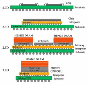
In electronic packaging technology, 2.0D, 2.5D, and 3.0D packaging differ significantly in physical structure, electrical connections, and integration density (see Table 1).
In addition, the industry includes subcategories such as 2.1D and 2.3D packaging, which this paper does not list in detail here.
The evolution from 2.0D to 3.0D packaging technology reflects a trend from planar integration to vertical stacking and from low density to ultra-high integration (see Figure 1).
| Packaging Type | Physical Structure | Electrical Connection | Integration, Performance, and Applications |
|---|---|---|---|
| 2.0D Packaging | All chips and passive components are directly mounted on the carrier board plane, with no stacking. | Circuits and vias on the carrier board provide electrical interconnection. Chips are usually connected to the carrier board by wire bonding. | Lowest integration level, mature technology, and low cost. Suitable for traditional consumer electronics and simple chips. |
| 2.5D Packaging | Chips are stacked or arranged side by side on an interposer with TSVs, providing inter-chip connectivity. | Electrical interconnection is achieved through micro-bumps and TSVs on the interposer. | Higher integration, higher I/O density, and lower transmission latency. Different functional chips can be efficiently integrated into one package. |
| 3.0D Packaging | Logic or memory bare dies are vertically stacked, with TSVs providing vertical interconnection between silicon dies. | Through-silicon vias (TSVs) or through-glass vias (TGVs) connect stacked chips, minimizing interconnection path lengths. | Highest integration level. Vertical interconnection provides higher bandwidth and lower power consumption, making it suitable for high-performance computing and storage applications. |
Table 1. Differences Between 2.0D, 2.5D, and 3.0D Packaging
2. Classification of IC Integration and Principles of Heterogeneous Integration
Integrated circuit packaging includes monolithic integration (MI), homogeneous integration (HOL), and heterogeneous integration (HI).
Monolithic integration refers to the packaging of a single chip;
Homogeneous integration refers to the packaging of multiple chips with identical structures or the fabrication of all components on the same material;
Heterogeneous integration, on the other hand, enables the integration of multiple dissimilar chips into a single package.
Advanced packaging technologies focus on heterogeneous integration. This technology enables the integration of small chips with diverse functions.
Typical chips include processors, memory units, and high-speed data transmission chips.
Engineers stack these functional chips in a building-block manner to form 3.0D packages (see Figure 2).
For heterogeneous integration, designers independently design and fabricate individual chips, then interconnect them through standard interfaces.
This improves signal routing and power distribution, thereby significantly enhancing system performance, bandwidth, and energy efficiency;
Reducing power consumption; optimizing thermal management; increasing yield;
And lowering costs—all while maintaining modularity and future scalability.
3. Application Value of Advanced Packaging for AI and HPC Systems
As process scaling approaches its physical limits, designs centered on a single large chip struggle to meet the demands of AI and HPC for high-speed computing, ultra-high bandwidth, and low power consumption.
The information technology sector’s reliance on central processing units (CPUs) has shifted toward graphics processing units (GPUs).
While CPU power consumption has largely plateaued, the new trend of pushing GPUs to the forefront of high-speed computing in data centers is also exacerbating the increase in power consumption.
Currently, a single GPU can operate at kilowatt-level power consumption, while a rack’s power consumption approaches or exceeds hundreds of kilowatts.
Due to the limitations of air cooling, accelerating application performance cannot rely solely on the chip;
Instead, it requires a redesign of the entire stack, including algorithms, software, and processors.
Against this backdrop, advanced packaging has become a key driver of sustained performance growth.
Today’s complex 2.5D and 3.0D architectures integrate multiple chips and high-bandwidth memory into a single package;
These approaches can significantly increase computing density and memory capacity (see Figure 3).
In fact, integration driven by advanced packaging has already achieved orders-of-magnitude growth in computing power and memory capacity, effectively extending and surpassing the traditional expectations of Moore’s Law.
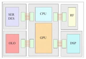
![Figure 3 Advanced packaging extends system scalability beyond the chip through disaggregated integration, thereby overcoming traditional node-level limitations and enabling miniaturization, scaling, and cross-scale architectures [1] (Source: Marvell Technology).](https://pcba-manufactory.com/wp-content/uploads/2026/10/Figure-3.webp "Figure 3 Advanced packaging extends system scalability beyond the chip through disaggregated integration, thereby overcoming traditional node-level limitations and enabling miniaturization, scaling, and cross-scale architectures [1] (Source: Marvell Technology).")
Examples of Advanced Packaging
Overview of Typical Mass-Production Advanced Packaging Technologies
Advanced packaging is a general term for innovative packaging models and is not limited to any single approach.
The author has recently compiled the following examples of advanced packaging.
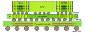
One of the advanced mass-production packaging technologies is TSMC’s Chip-on-Wafer-on-Substrate (CoWoS) packaging.
It achieves high-density integration of GPU chips and high-bandwidth memory (HBM) through the fine-pitch interconnects of the adapter board and the substrate (see Figure 4).
This method is widely adopted in AI accelerators, offering an appropriate balance between cost, package size, and manufacturing complexity.
The industry has recently proposed a novel “chip on wafer on PCB” (CoWoP) packaging approach.
This method attaches chips with redistribution layers (RDL) to an interposer and then directly mounts them onto UHDI PCBs.
Composite Stacking Packaging Technology of Intel
Intel’s Embedded Multi-Die Interconnect Bridge (EMIB) packaging integrates a silicon bridge within an organic substrate to enable high-density inter-die connections without the need for a stacker (see Figure 5), thereby reducing costs, improving scalability, and preserving high-bandwidth links in the target area.
Meanwhile, the industry integrates Intel’s EMIB packaging with Foveros packaging technologies (see Figure 6).
Foveros packaging technology introduces a 3.0D stacked design that stacks and connects different logic chips, which is a key technology for heterogeneous integrated chips.
Designers partition traditional large-scale chips into multiple smaller chip units. This approach integrates discrete functional modules into a monolithic integrated structure.
It meets the design demands for diverse applications, power consumption standards, and form factors.
This technique delivers enhanced, customizable performance while lowering overall costs.
Furthermore, researchers have gradually introduced glass substrate technology into this field.
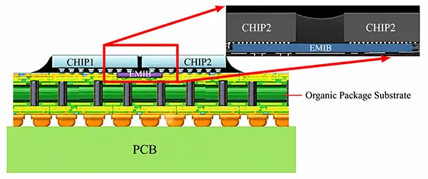
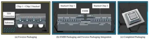
Figure 6 Foveros and EMIB packaging architectures
Ultra-High-Density Fan-Out Packaging Solution
Fan-out packaging, which provides greater flexibility in chip placement by directly integrating multiple RDL input/output connections onto the package.
For example, Changjiang Electronics Technology’s full series of XDFOI ultra-high-density fan-out packaging solutions represents a new type of silicon-free through-hole wafer-level ultra-high-density packaging technology:
This solution features multiple wiring layers with a line width/spacing of 2 μm and employs ultra-narrow-pitch bump interconnect technology.
With its large package size, it can integrate multiple chips, high-bandwidth memory, and passive components, allowing different functional devices to be consolidated into a system-in-package (SiP).
This significantly reduces system costs and shrinks package size, making the solution suitable for a wide range of applications.
Co-Packaged Optics Technology for High-Speed Interconnection
Rising demands for ultra-high-speed interconnects drive the widespread adoption of optical interconnects.
This technology integrates optical and electronic components into a single module (see Figure 7), forming the co-packaged optics (CPO) architecture.
By integrating optical components directly with silicon, CPO minimizes signal loss and power consumption while significantly improving bandwidth and energy efficiency.
For example, Changjiang Electronics Technology has achieved key breakthroughs in CPO technology.
Its high-density fan-out packaging (XDFOI) technology is a solution specifically designed for chiplet architectures.
It innovatively integrates optoelectronic devices with logic chips into a single package, thereby restructuring the optical signal transmission path at the physical level to effectively reduce system-level interconnect losses.
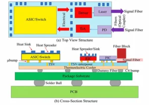
Next-Generation Panel-Level Packaging Technology
As the complexity of AI servers and HPC equipment continues to increase, large-area panel-level packaging represents yet another innovation to support the roadmap toward a trillion-transistor system-level packaging architecture.
ASE has developed an automated production line for 310 mm × 310 mm panel-level packaging, offering 2 µm × 2 µm line width/line spacing capabilities and spatial capacity.
The transition from traditional circular wafers to rectangular panels allows for more chips to be placed per unit, thereby improving material utilization.
Larger panels support higher throughput and shorter cycle times while integrating increasingly complex multi-chip architectures.
TSMC is advancing panel-level packaging, which it has named CoPoS (chip-on-panel-on-substrate). CoPoS replaces the wafer in CoWoS with a panel (Panel)
in place of the wafer used in CoWoS, enabling a larger packaging area, which in turn boosts production efficiency and reduces manufacturing costs.
Industrial Standardization and Technical Advantages of Panel Packaging
The entire industry, including Intel and Samsung, is currently moving toward panel standardization, with mainstream sizes including 310 mm × 310 mm, 510 mm × 515 mm, 600 mm × 600 mm, and other specifications.
Unlike traditional circular wafer packaging, panel-level packaging employs a rectangular layout.
To minimize expansion, contraction, and warping in large-size panels, the industry is exploring the use of glass substrates to overcome the physical limitations of organic and silicon substrates while increasing chip density.
This approach is regarded as a key candidate technology for next-generation advanced packaging.
Connotation and Technical Value of Tao Law
On May 26, 2026, numerous media outlets reported that Huawei had proposed a new principle to guide the development of the semiconductor industry—Tao (τ) Law.
The core of Tao Law is to replace “geometric scaling” with “time scaling.”;
By continuously reducing signal propagation delay through innovative technologies such as logic folding, it enhances transistor density and system performance.
From a system integration perspective, Tao’s Law introduces logic folding technology.
By distributing circuits across multiple layers of vertically stacked active chips, it shortens the trace length of the critical path, thereby enhancing chip performance.
It can be said that Tao’s Law combines heterogeneous integration and 3.0D packaging technology to optimize the technical path from the perspective of advanced packaging, serving as the physical means to achieve “time miniaturization.”
Impact of Advanced Packaging on the Electronic Circuit Industry
The Blurring Boundaries Between Chips, Packaging, and Circuit Boards
1. Holistic Multi-Physical Field Requirements for Advanced Packaging
Advanced packaging is not merely a three-dimensional interconnect technology;
It involves the close coupling of structural integrity, signal integrity, power integrity, and thermal performance.
Addressing this complexity requires a holistic approach that considers chips, packaging substrates, and circuit boards—from systematic co-design to physical implementation—all of which are critical.
From the perspective of electronic system technology, chip packaging must have a carrier or substrate, and the installation of ICs or module components requires a printed circuit board;
Electronic circuit technology plays a critical role.
Traditional electronic assembly processes consist of chip fabrication, packaging, and testing, with IC and component assembly carried out sequentially.
However, in today’s AI environment, silicon chips, packages, and printed circuit boards form an extremely complex network of mechanical constraints, signal connections, and thermal solutions that cannot be addressed in isolation.
Consequently, the entire technology stack has become systematized, with upstream and downstream processes closely interconnected and even interpenetrating.
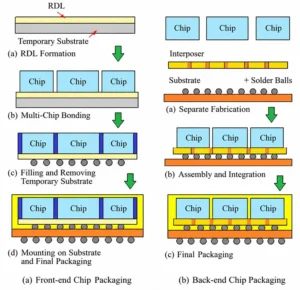
Currently, some advanced packaging processes typically involve manufacturing the chip and the carrier substrate separately.
These are then brought together at a packaging and testing facility to complete the packaging and form an IC, as shown in Figure 8.
In this process, the chip is first secured, and then I/O leads are attached to form the carrier substrate.
Since this packaging process is simultaneously the carrier substrate fabrication process, it tends to blur the boundaries between the chip, the package, and the circuit board.
2. New Integration Forms of Embedded Components and Additive Manufacturing
The structure of components embedded within a circuit board includes passive components (C, R, L, etc.) and active components (ICs or bare chips);
This not only increases the component density on the PCB but also shortens signal paths, thereby improving the board’s electrical performance and overall reliability.
It also incorporates heterogeneous integration and 3D structures, equivalent to system-in-package (SiP) technology.
Furthermore, additive manufacturing (AM) via 3D printing can combine multiple materials in multiple layers to form circuit modules containing electronic components.
For example, in-mold electronics (IME) technology integrates printed circuits, mounted components, and chips with injection molding processes to create functional electronic circuit modules;
The demand for ultra-high-speed interconnects is driving the adoption of optical interconnects, in which optical and electronic components are integrated and packaged into a single module, known as a CPO module.
With the development of HDI/UHDI technologies, carrier boards and UHDI board technologies are converging, and PCBs have evolved from traditional circuit carriers into key platforms for heterogeneous integration.
3. The Central Role of PCB in Advanced Packaging Ecosystem
PCB manufacturers with specialized UHDI expertise are discovering opportunities to enter the advanced packaging market, while semiconductor companies are also exploring carrier substrate manufacturing and direct packaging.
For example, chips on wafers are mounted on carrier substrates via adapter boards or directly onto PCBs, thereby creating a new electronic ecosystem comprising “semiconductor chips + advanced packaging + circuit boards.”
In the integration of these electronic functional systems, it is the circuit board that bridges the gap between components and houses them.
While designing and manufacturing a single chip or component is relatively straightforward, it is the interconnecting circuits (and optical paths) that enable the system to function as intended; thus, the circuit board plays a central role in the system.
Current advanced packaging, through innovative packaging processes and structural designs, can integrate multiple chips into a single system, encompassing 2.5D to 3.0D and heterogeneous integration system architectures.
Different advanced packaging structures are achieved through carrier boards or combinations involving adapter boards, RDL, and other components.
4. Policy Support for Packaging Substrates and PCB Industry
In the past two years, both the U.S. Congress and the European Union have passed “Semiconductor Chips Acts” to encourage and support the domestic development of the chip manufacturing industry, which includes promoting the development of packaging substrates and PCBs.
These acts extend support from semiconductors to strategic areas such as PCBs and PCBA, because chips cannot float in the air—they can only function when mounted on substrates and PCBs.
Advances in Electronic Circuit Technology
1. Substrate and Printed Circuit Board Technology
1) Structural Features and Fabrication Processes of High-End IC Packaging Substrates
IC packaging substrates are designed to support more chiplets on a smaller board area and integrate more components with different functions to form high-performance modules.
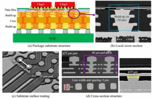
As shown in Figure 9, the industry is moving toward high-tier UHDI board structures, which feature large cell sizes, high layer counts, and fine traces.
Interconnections utilize fine-pitch flip-chip mounting, with bumps or copper pillars enabling even smaller pitch dimensions: 40 μm pitch, 25 μm pad size, 10 μm via diameter, and 2 μm trace width/spacing.
Manufacturing processes for advanced packaging substrates are similar to those for UHDI boards, including the semi-additive process (SAP) and the modified semi-additive process (mSAP);
The traditional subtractive method (copper foil etching) is no longer suitable.
Microconductive blind via processing faces challenges such as increasingly smaller blind via pads and via diameters, a wide variety of substrate materials, and constantly evolving laser sources.
In current PCB mass production, CO₂ and UV nanosecond lasers remain the industry standard for high-throughput production;
However, as product designs continue to shrink and materials become increasingly sensitive, picosecond technology is being adopted more and more widely.
This technology involves a combination of UV or picosecond lasers with CO₂ lasers, achieving a perfect balance of high precision and high throughput.
2) Laser Drilling Technologies for Glass TGV Substrates
In addition, femtosecond lasers utilizing ultrashort-pulse cold processing are also being applied in research and development as well as in ultra-high-end semiconductor advanced packaging applications.
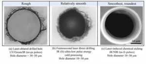
For laser drilling of TGVs on glass substrates, the methods can be broadly categorized into UV laser ablation drilling, femtosecond laser direct drilling, and laser-induced deep etching (LIDE).
These three methods differ in terms of processing mechanisms, hole quality, and throughput (see Figure 10), with LIDE offering the highest throughput and best quality, making it ideal for subsequent metallization of the holes.
3) Ultra-Fine Machining Capability of Ultrashort-Pulse Lasers on Glass Substrates
There are already examples of ultra-fine drilling on glass substrates using 1.5 ps ultrashort-pulse lasers in the deep ultraviolet region.
These lasers have successfully drilled holes with diameters smaller than 10 μm in 0.2 mm-thick glass plates and have even achieved ultra-high AR (aspect ratio) holes with a depth of 1 mm and a diameter of 3 µm.
Glass TGV substrates are fabricated using electroless copper plating, vapor deposition, or sputtered metal seed layers, enabling the creation of fine patterns with a line width/spacing (L/S) of 5/5 μm;
Glass interconnect substrates can even achieve an L/S of 2/2 μm.
2. Materials and Equipment Technology
1) Material Performance Requirements and CTE Matching of IC Carrier Substrates
The substrate is a key factor in the performance and reliability of IC carrier boards.
In addition to possessing electrical properties—such as low dielectric constant and low dielectric loss—similar to those of high-end PCBs, advanced packaging carrier boards must also feature thinner substrates to facilitate the development of lighter, thinner multi-layer carrier boards; Heat is becoming a critical factor.
High-performance packaging requires excellent thermal resistance, dimensional stability, and warpage resistance.
It is necessary to consider the differences in the coefficient of thermal expansion (CTE) of different materials.
These materials include insulating dielectric layers, conductor layers and solder.
Reasonable CTE matching with silicon chips is essential. This effective matching avoids internal cracking failures of packaging structures.
Substrates used for IC carrier boards and adapter boards include organic substrates, silicon substrates, glass substrates, and ceramic substrates; performance, reliability, and cost must be considered when making a selection.
Organic substrates are low-cost and offer better CTE matching with the carrier, but they have low thermal conductivity; a typical organic resin is bis-maleimide-triazine.
Silicon substrates have excellent electrical properties and thermal conductivity, but they are expensive and prone to warping.
Glass substrates have excellent electrical properties and a CTE closer to that of silicon, but they are highly brittle and difficult to process;
Ceramic substrates have a coefficient of thermal expansion (CTE) similar to that of silicon, resulting in minimal thermal expansion differences between the substrate and the chip, which helps suppress warpage.
They also offer excellent heat resistance; however, their drawbacks include high brittleness and poor processability.
2) Dielectric Films and Conductive Filling Technology for Ultra-Thin Substrates
Both advanced packaging substrates and interposers require thin and lightweight designs, and in the lamination process, glass-fiber-reinforced prepregs used as insulating layers
are no longer suitable. The use of laminated films without glass cloth reinforcement is gradually increasing, with ABF being a typical laminated insulating material.
Currently, ABF comes in a variety of forms; for example, photoresist-type insulating dielectric films feature low Dk, low Df, low CTE, and excellent thermomechanical stability;
Photoresist-type polyimide films can be laminated as smoothly as photoresist dry films onto large-area substrates;
Through exposure and development, they produce microscopic blind vias, forming microvias smaller than 10 µm—a process more efficient than laser drilling.
Even at a film thickness of 10 µm, it reliably achieves ultra-small microvias of 6 µm.
Currently, copper electroplating is one of the mainstream solutions for TGV commercialization;
However, this technology suffers from issues such as lengthy processing times and a tendency for cracks to form within the through-holes.
Consequently, conductive paste filling technology has gained significant attention, and new advancements in the development of copper pastes for TGVs are continuously being made.
The newly developed copper paste for glass through-holes exhibits electrical conductivity comparable to that of an electroplated copper layer and can be directly filled into the through-holes.
Compared to existing electrolytic copper plating, this new technology reduces process time to approximately one-fifth while also minimizing the risk of glass breakage.
3) Precision Equipment Supporting Advanced Packaging Substrate Manufacturing
In terms of specialized equipment, to meet increasingly stringent precision requirements, direct laser imaging equipment has become indispensable in pattern fabrication;
It features automatic positioning and compensation functions and offers high resolution.
For example, if the minimum line width on an IC substrate is 2 μm, the equipment must achieve an alignment accuracy of ±1 μm at a minimum line width of 1 μm.
Laser drilling machines require different laser source configurations to accommodate the drilling requirements of various substrates.
Wet processing equipment—such as that used for direct metallization of via lines, plating lines, and etching lines—requires intelligent control and automated chemical addition and compensation, including proper waste recovery and reuse as well as green manufacturing practices.
Inspection equipment must be equipped with high-resolution automated optical inspection (AOI) systems and precision fly-probe testers for fine-pitch circuits.
For example, probe testers must be large in size, fast, efficient, and capable of high throughput, while also being suitable for high-density applications (such as interconnect pads measuring 10 µm with a pitch of 25 µm).
They must also offer Kelvin (4-wire), buried resistor/capacitor, and withstand voltage testing options, as well as X-ray and CT non-destructive testing (NDT) equipment, scanning electron microscopes (SEM), and energy dispersive spectrometers (EDS).
4) Coordinated Development of the Whole Industrial Chain
In summary, to meet the demands of advanced packaging, both packaging substrate and PCB technologies will be elevated to new heights, and products, materials, equipment, and even the entire industrial chain must develop in tandem.
Conclusion
At this stage, the cutting edge of electronic packaging lies in 3D stacking and heterogeneous integration, with packaging gradually evolving into a system in its own right.
Advanced packaging is opening up new pathways for the development of the electronic circuit industry.
To this end, we must understand what advanced packaging is and how the electronic circuit industry can meet its requirements.
Only by doing so can we stride forward confidently on this new path. I hope this article provides some insights for industry professionals.

