
What is the difference between a PCB and an ABF substrate? Let’s clarify this here: A PCB is a “system-level” board that connects components such as resistors, capacitors, and chips into a functional circuit;
An ABF substrate is a “chip-level” board whose function is to attach a bare chip to a PCB.
The former operates at the millimeter scale, while the latter operates at the micrometer scale;
Furthermore, they are not upstream and downstream processes but rather two distinct branches of the industry.
Two “Boards” Are Different: One Operates at the System Level, the Other at the Chip Level
PCB (Printed Circuit Board): A finished electronic component made by processing copper foil on a substrate (such as laminated copper board) to form circuits and pads, drilling holes to connect layers, and applying solder mask.
PCBs serve to carry and interconnect diverse electronic components.
As a fundamental electronic carrier, a PCB supports the surface soldering of various components such as chips, capacitors, and connectors.
It electrically interconnects these components to form a complete circuit in accordance with circuit schematics.
The finished PCBs are ultimately integrated into electronic devices including mobile phones, servers, and switches.
It operates on a millimeter scale: typical trace widths and spacing are 50 µm or greater, through-hole diameters are approximately 200 µm, and the number of layers typically ranges from 4 to 16.
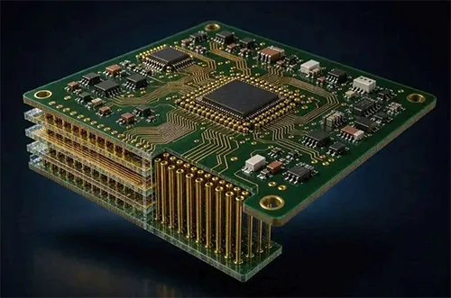
Key Features: ABF substrate services a bare chip.
Chip bump pitch typically ranges from tens to more than one hundred micrometers.
In contrast, the ball pitch of conventional PCBs falls within the millimeter scale, creating a nearly 100-fold dimensional gap.
Packaging substrates serve as a critical intermediate medium to bridge this significant scale difference.
The top substrate layer adopts micrometer-scale ultra-fine circuit lines to fan out dense chip bumps.
Correspondingly, the bottom layer scales up the interconnection structure to millimeter-scale solder balls, enabling reliable electrical connection and signal transmission between the chip and the external PCB.
It operates at the micrometer scale: line widths and spacings can reach 5–10 μm, with advanced products pushing toward 2–3 μm; microvia diameters are only 30–50 μm;
And the number of stacked layers can exceed 20. It is important to distinguish between two types of packaging: in general-purpose FC-BGA, the chip is directly flip-mounted onto the carrier board;
Whereas AIGPU uses CoWoS packaging, which involves a silicon interposer sandwiched between the chip and the carrier board—the carrier board actually supports the entire “chip + interposer” assembly.
Key Differences: A Single Table That Clarifies Everything
Fundamental NatureA chip-level interconnection carrier within semiconductor packaging.A system-level finished component that carries electronic components in a complete device.
| Dimension | ABF Substrate (IC Packaging Substrate) | PCB (Printed Circuit Board) |
|---|---|---|
| Target Application | A single bare chip (CPU / GPU / AI accelerator chip). | Discrete components such as resistors, capacitors, connectors, and packaged chips. |
| Line Width / Spacing | 5–10 μm, advancing toward 2–3 μm in high-end products. | Typically ≥50 μm; ≥30 μm for advanced multilayer boards. |
| Via Diameter | Laser-drilled microvias: 30–50 μm. | Mechanically drilled vias: approximately 200 μm. |
| Layer Count | Typically 8–20 layers or more, with increasing layer counts in advanced products. | Commonly 4–16 layers; AI server boards may exceed 20 layers. |
| Main Manufacturing Process | Semi-additive process (SAP / mSAP): first deposit a thin copper seed layer, then electroplate copper to build circuit traces. | Subtractive process: etch away excess copper from a copper-clad board, leaving the required circuit traces. |
| Base Material | ABF build-up film (glass-fiber-free resin film) and BT resin. | Copper-clad laminate (fiberglass fabric + resin + copper foil). |
| Core Function | Dimensional conversion: transforms micrometer-scale chip pads into millimeter-scale solder ball connections. | System integration: electrically connects electronic components according to the circuit design. |
| Manufacturing Difficulty & Profitability | Semiconductor-grade cleanliness and process control; gross profit margins are often 30%–50%. | Mature manufacturing processes; gross profit margins are generally below 15%. |
| Domestic Production / Localization | Low localization rate; domestic production accounts for less than 10% of global output, with ongoing efforts to catch up. | High localization rate; Chinese manufacturers are among the world’s leading producers by capacity. |
Note: The technical specifications and profitability figures are translated from the original image. Actual values vary by manufacturer, technology, and product category.
Three common misconceptions correspond to three distinct boundaries:
Misconception 1: “An ABF substrate is simply a higher-end PCB.”
This is inaccurate—the two differ in process (semi-additive vs. subtractive), materials (ABF film vs. copper-clad laminate), equipment, and customer base;
They are also categorized separately in industry statistics. It is a distinct product category, not a tier within the PCB hierarchy.
Misconception 2: “Substrates are upstream raw materials for PCBs.” Incorrect—copper-clad laminate is the raw material for PCBs;
Substrate boards are not supplied to PCB manufacturers. Instead, they are assembled with chips; after packaging, the entire assembly is soldered onto the PCB.
Misconception 3: “A substrate board is an ABF substrate board.” Substrate boards fall into two major material categories: BT and ABF.
ABF supports finer line widths (approximately 5 µm, compared with roughly 15 µm for BT).
It is mainly adopted for high-computing-power chips, whereas BT substrates are widely used in memory and RF packaging applications.
Root of the Difference
One “etches” the circuit patterns, while the other “grows” them.
The manufacturing process is the clearest distinction between the two.
PCBs use a subtractive process: Copper foil is initially laid over the entire surface;
Unwanted regions are covered by photoresist, and the remaining copper is removed via chemical etching.
The formed circuit is fabricated using the subtractive process.
Etching inevitably introduces side etching effects; the finer the line width, the more difficult the control.
Therefore, it is generally cost-effective to produce lines down to the 50 µm range.
ABF substrates use a semi-additive process (SAP/mSAP): An extremely thin seed copper layer is first chemically deposited onto the insulating ABF film;
Next, we electroplate the trace-forming regions to thicken the copper layer and ultimately flash-etch the excess seed layer, which constitutes the additive process.
This results in steeper sidewalls and better control over line width, making the 5–10 µm range achievable.
Interlayer interconnects also differ: PCBs rely on mechanical drilling followed by copper plating on the hole walls, while ABF substrates use UV lasers to create 30–50 µm microvias, which are then filled via electroplating.
In terms of materials, these are also two distinct systems.
Traditional PCB substrates adopt resin-impregnated glass fiber cloth as the base material, with copper foil laminated on both sides.
In contrast, ABF substrates adopt glass-fiber-free resin films as their interlayer dielectric material.
This dielectric film must possess a coefficient of thermal expansion matching that of silicon, which is approximately 2.6 ppm/°C.
Without such matching thermal expansion characteristics, repeated thermal cycles during chip operation will induce cracks in solder joints.
It must also have low dielectric loss to support high-speed signals.
This accounts for the fact that mature PCB lamination and etching production lines are not applicable for manufacturing carrier substrates.
Let’s now look at how the interior of a carrier substrate is “built up.”
It is not a uniform stack: the typical structure consists of “top and bottom ABF layers sandwiching a glass-fiber-reinforced core layer.”
The core layer of the packaging substrate undertakes key structural functions, providing reliable mechanical support and stable dimensional performance.
The stacked laminated layers are responsible for constructing ultra-fine circuit structures for signal transmission.
Different from traditional structural designs, high-end packaging substrates adopt a coreless structure.
This design removes the conventional core layer and solely relies on laminated layers for structural and circuit integration.
It effectively reduces substrate thickness and delivers excellent electrical properties for high-end chip packaging applications.
Furthermore, the so-called “20 layers” do not simply mean gluing 20 separate boards together;
Rather, they are built up by repeating the process of “laminating ABF film, UV laser drilling, chemical copper plating, and electroplating” about twenty times on a single board.
The higher the number of layers, the harder it is to maintain yield rates—which is precisely why it takes two to three years to ramp up production capacity.
Position in the Industry Chain: Sandwiched Between the Chip and the Motherboard
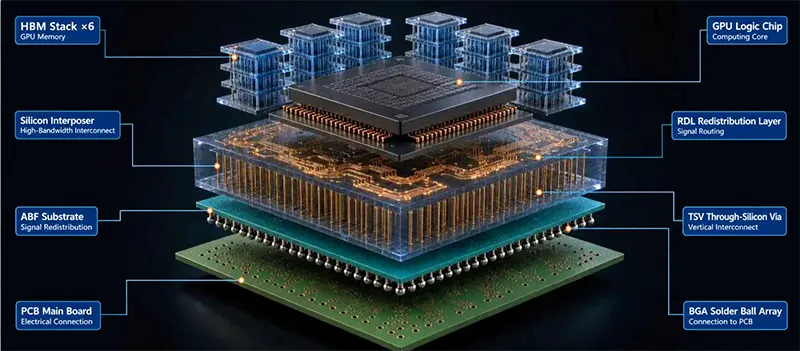
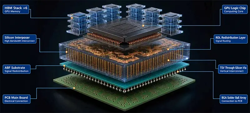
If you cut an AI accelerator chip package open from top to bottom, the layers are as follows:
At the topmost layer lie the bare GPU die and the adjacent HBM stack, which are first bonded to a silicon interposer.
The interposer is subsequently attached to the packaging substrate (also referred to as the ABF substrate) through micro-bumps.
The bottom side of the substrate carries a BGA ball array that is soldered to the main PCB.
Once you understand this chain, it becomes clear: the ABF substrate occupies the middle link in the “chip-to-package-to-system” chain, connecting to micron-level chip interconnects above and millimeter-level board-level components below.
Therefore, the relationship between the two is not one of “who supplies what to whom,” but rather each handles its own segment:
The carrier tube expands the chip’s bump pitch—just over 100 µm—into a ball pitch of around 1 mm on the carrier board’s bottom surface;
The PCB then connects this packaged chip with memory, power supply, and interfaces to form a functional device.
Why It Matters: The Layer with the Highest Value Is Also the Most Challenging to Produce
Quantifying Value First: In high-end flip-chip (FC) packaging, substrate costs account for 70 to 80 percent of total packaging material costs;
Gross profit margins for substrate manufacturing typically range from 30 to 50 percent, while those for PCBs generally remain below 15 percent.
As AI chips grow larger and feature more pins, value increasingly concentrates in the substrate layer.
In terms of market potential, China’s IC packaging substrate market is forecast to expand from USD 3.15 billion in 2025 to USD 5.63 billion in 2030, corresponding to a compound annual growth rate (CAGR) of roughly 12.3%.
The ABF substrate industry faces a severe supply shortage.
The supply-demand gap for high-end ABF substrates is estimated at 20%–40%, triggering a sharp price rise within a single year.
Additionally, capacity expansion of high-end production lines involves a long industrial cycle.
The whole process, including plant construction, equipment commissioning and yield stabilization, requires 2.5 to 3 years.
Core production equipment, such as laser drilling devices and high-precision exposure systems, features even longer delivery lead times, further restricting rapid capacity growth.
Opportunities and Risks: The Shortage Is Real, and the Uphill Battle Is Real
From the perspective of industrial research institutions, the booming production of AI computing chips has reshaped the supply structure of advanced packaging materials.
Multiple institutional forecasts indicate that packaging substrates have become the most bottlenecked and scarce component in advanced packaging processes.
The mismatched relationship between tight market supply and lengthy capacity expansion cycles constitutes the core industrial contradiction restricting the large-scale development of high-end AI chip packaging.
Author’s Analysis: The fundamental bottleneck of the substrate supply chain does not lie in basic production feasibility.
Instead, it focuses on the capability of stable, large-scale and high-yield mass production.
Substrate products require lengthy customer certification procedures and exhibit a slow yield ramp-up process.
In addition, raw material preparation faces prominent technical challenges in maintaining consistent batch quality, further restricting stable capacity release.
Therefore, technological progress should be evaluated on an annual basis rather than linearly extrapolated from monthly data.
The potential risks and uncertainties are specified below in three traceable items:
1. High concentration in upstream materials: Ajinomoto holds the majority of the global market share for ABF film.
Quotas, prices, and geopolitical disruptions will directly impact substrate manufacturers’ costs and production schedules (publicly available data allows for tracking of upstream supply dynamics);
2. Pace of domestic substitution: China’s share of the global substrate market remains below 10 percent;
Yield rates and batch consistency lag behind those of leading overseas manufacturers, and lengthy customer certification cycles may result in a slower ramp-up than market expectations;
3. Technological route evolution: If new substrate technologies, such as glass substrates, mature more rapidly, they could disrupt the long-term demand landscape for ABF substrates.

