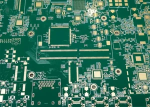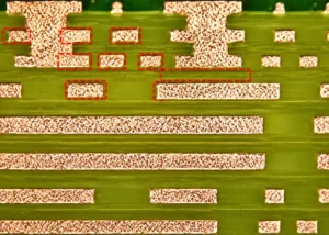
High-end automotive electronics, AI accelerator cards and high-power modules develop rapidly. This trend pushes PCB products to upgrade their electrical and thermal performance.
Key targets include higher current-carrying capacity, improved thermal conductivity and better heat dissipation.
Designers find conventional micro-blind via structures constrained by the cross-sectional area of the via, so these structures show obvious shortcomings in electrical conductivity and thermal conductivity;
They are no longer suitable for the operating conditions of high-power devices. Currently, the PCB industry offers an increasingly diverse range of design solutions and manufacturing processes for large-diameter blind vias;
However, there are significant differences in formation quality and production yield among different process routes.
This paper carries out comparative tests on two mainstream laser processes for large blind vias. The first scheme uses CO₂ laser direct drilling (LDD) followed by laser reaming.
Researchers verify its performance using optimized stack ratio parameters. The second scheme adopts a hybrid workflow. The process first applies chemical etching to form a conformal mask (CFM).
It then carries out CO₂ laser ablation to define blind vias. By comparing the processing results of these two methods, this study aims to provide a technical basis for selecting mass production processes for large blind holes in high-power PCBs.
Principles of Blind Hole Machining
The CO₂ laser direct drilling process tunes core parameters. These parameters include mask diameter, laser energy, pulse width, and pulse number.
The process runs in sequence over the target blind via region. It removes copper, trims the hole contour, and strips residual adhesive.
For large blind holes with a diameter of ≥0.25 mm, we must adopt a ring-shaped enlargement mode to match the corresponding hole overlap ratio.
This involves scanning in multiple concentric rings layer by layer to ensure the laser processing path completely covers the entire area of the large blind hole, forming the blind hole through laser ablation, as shown in Figure 1 (a).
The CFM pretreatment + laser drilling hybrid process is a staged manufacturing process involving etching to create windows followed by laser drilling.
First, we apply etching pretreatment to the sheet to precisely etch the contour dimensions of the target large blind holes;
Then, we use a laser drilling machine to perform stacked-hole drilling. During this stage, we must reserve a compliant safety margin for stacked holes to prevent drilling misalignment.
The process is shown in Figure 1 (b).
Experimental Section
Materials and Equipment
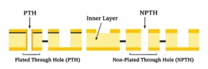
Materials: Test specimens (basic information shown in Figure 2), electroplating solution (vertical direct-current electroplating solution, primarily containing Cu²⁺, H₂SO₄, Cl⁻, accelerators, leveling agents, brighteners, etc.).
Equipment: We perform laser drilling with a Mitsubishi CO₂ laser drilling machine, a vertical DC electroplating line, a tin-plating furnace, a reflow soldering machine, a multimeter, a microtome, a metallographic microscope, and other equipment.
Test Procedure
1. Process Flow
LDD Blind Via Process: Sheet Cutting → Inner Layer Traces → Laminating → X-ray Drilling → Trimming and Grinding → Laser Browning → CO₂ Laser Drilling → Film Stripping → Laser Automated Optical Inspection (Laser AOI) → Mechanical Drilling → Vertical Copper Plating → Vertical Board Plating → Vacuum Resin Via Filling → Via Filling AOI → Horizontal Resin Removal → Horizontal Copper Plating → VCP Through-Hole Plating → Outer Layer Traces (Pre-treatment → Film Application → Exposure → Development → Etching → Film Removal) → Subsequent Processes;
CFM + Laser Blind Hole Drilling Process: Material Cutting → Inner Layer Traces → Laminating → X-ray Drilling → Trimming and Grinding → Mask Window Opening (Pre-treatment → Film Application → Exposure → Development → Etching → Film Removal) → CO₂ laser drilling → Laser AOI → Mechanical drilling → Vertical electroless copper plating → Vertical board plating → Vacuum resin via filling → Via filling AOI → Horizontal resist removal → Horizontal electroless copper plating → Vertical continuous via plating (VCP) → Outer layer circuits (pre-treatment → film application → exposure → development → etching → film removal) → subsequent processes.
2. Test Protocol
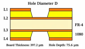
The PCB stack-up design is shown in Figure 2.
Specifically:
- blind via diameter D1 = 250 μm, aspect ratio AR1 = 0.3:1;
- D2 = 300 μm, AR2 = 0.25:1;
- D3 = 350 μm, AR3 = 0.22:1;
- D4 = 400 μm, aspect ratio AR4 = 0.19:1;
- D5 = 500 μm, aspect ratio AR5 = 0.15:1.
We compared two processing approaches in the test. The first is CO₂ laser direct window drilling with a fixed 50% hole stacking ratio.
The second is laser drilling after window formation by etching. Figure 3 illustrates both processes.
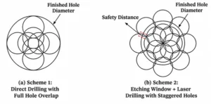
(1) Option 1: For all five blind via specifications from L1 to L2, we arranged the via patterns uniformly with a standard 50% via overlap rate.
We completed blind via processing by a single-pass direct cutting process with a CO₂ laser, and this group serves as the reference control group for this experiment;
(2) Scheme 2: First-order blind vias in L1–L2 were fabricated using the CFM conformal mask process.
First, we pre-fabricate a copper window mask that matches the specifications in the blind-via regions using outer-layer negative film pattern transfer and etching processes.
The outer-layer copper foil served as the laser shielding boundary.
After completing the CFM pretreatment, we formed the blind vias with a CO₂ laser using appropriate process parameters.
3. Blind Hole Reliability Testing
We conducted reliability testing on fully processed test boards in accordance with the IPC-TM-650 test specification.
Test items included: 3 thermal stress tests, as well as 5 and 10 lead-free reflow soldering tests.
After finishing all tests, we performed visual inspections and metallographic section analyses on the five types of blind vias on each board.
We also collected data on resistance change rate after thermal stress testing and lead-free reflow soldering to comprehensively evaluate sample reliability.
Specific test items, test conditions, and evaluation criteria are shown in Table 1.
| Test Item | Test Conditions and Methods | Acceptance Criteria |
|---|---|---|
| Thermal Stress | Temperature: (288 ± 5) °C; Duration: 10–11 s; Solder Floating: 3 times | No abnormalities such as blistering or solder mask peeling on the surface. |
| Lead-Free Reflow Soldering | (1) Perform open-circuit and short-circuit tests on the circuit network. (2) Perform a double 85 test for 12 hours. (3) Maximum reflow soldering temperature: 260 °C; 3 cycles. | After testing, no cracks in the via walls, no delamination of the substrate, and no microcracks at the bottom of the microvias. Resistance change after testing must be less than 10%. |
Table 1. L1–L2 Blind Via Reliability Test Items, Conditions, and Acceptance Criteria
Analysis and Discussion of Test Results
Blind Hole Machining Results for Different Test Protocols
1. Test Specimen and Experimental Scheme
The test specimens featured five sets of first-order blind holes with diameters of 250, 300, 350, 400, and 500 μm, all with a uniform depth of 75.6 μm. Conventional prepreg (PP) was used.
Technicians employed two processing methods in the experiment: direct laser drilling and a combination of CFM windowing and laser drilling.
They fabricated blind holes by optimizing process parameters. After resin plugging and DC electroplating, technicians sectioned the molded specimens for metallographic examination.
The examination included hole profile, upper-to-lower diameter ratio, copper layer thickness on the hole walls, and overhanging copper dimensions.
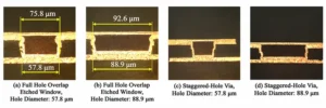
The microstructural morphology is shown in Figure 4.
2. General Inspection Results of Blind Vias
Technicians measured the cross-section samples dimensionally at the same time.
They collected data including the top-to-bottom diameter ratio and hole-wall copper thickness for each group of blind vias.
Cross-sectional morphology and measurement data show consistent results for both processes. No resin residue remains at the bottom of the blind vias. The bottom copper layer suffers no breakdown damage.
All holes present regular inverted trapezoidal profiles. The top-to-bottom diameter ratio of every blind via exceeds 90%. Hole-wall copper thickness is above 13 μm.
We control the overhang copper size within 15 μm for all samples. All indicators met the requirements of relevant standards.
3. Performance Comparison of the Two Drilling Processes
Comparing the test results of the two processing methods, the upper-to-lower diameter ratio was higher for the CFM windowing + laser drilling process than for the direct laser drilling process.
Both sample groups share the same electroplating procedure and parameters. The comparison of copper overhang demonstrates that the CFM windowing plus laser drilling process yields smaller overhang than direct laser drilling.
This study conducted dimensional measurements and a comparative analysis of cross-sectional specimens produced using two blind hole machining methods; the test data are shown in Table 2.
4. Comprehensive Evaluation and Conclusion
Data analysis reveals the following differences. Laser direct drilling produces blind vias with a larger gap between measured diameter and designed diameter.
In contrast, the process combining CFM etching windowing and laser drilling achieves better-controlled copper overhang.
Overall, both processing methods can achieve the target hole diameter requirements and meet the needs of actual production applications;
Among them, we can stably control the overhanging copper thickness of blind holes produced by the CFM etching combined with laser drilling process within 10 μm.
The CFM windowing plus laser drilling process outperforms direct laser drilling.
It achieves better results in hole profile, hole-wall surface quality, consistency of top-to-bottom diameter ratio, and dimensional deviation between finished and designed hole diameters.
| Process | Designed Hole Diameter (μm) | Measured Hole Diameter (μm) | Deviation (μm) | Deviation (%) | Microsection Top Hole Diameter (μm) | Microsection Bottom Hole Diameter (μm) | Bottom-to-Top Diameter Ratio (%) | Overhang (μm) | Result |
|---|---|---|---|---|---|---|---|---|---|
| LDD Blind Via | 250 | 238.096 | −11.904 | −4.76 | 255.19 | 235.61 | 92 | 12.680 | Pass |
| LDD Blind Via | 350 | 338.12 | −11.880 | −3.39 | 252.06 | 333.23 | 95 | 10.475 | Pass |
| LDD Blind Via | 500 | 487.253 | −12.747 | −2.55 | 507.25 | 487.45 | 96 | 11.135 | Pass |
| CFM + Laser Drilling | 250 | 254.061 | 4.061 | 1.62 | 257.05 | 231.35 | 90 | 5.225 | Pass |
| CFM + Laser Drilling | 350 | 355.434 | 5.434 | 1.55 | 354.54 | 329.25 | 93 | 5.460 | Pass |
| CFM + Laser Drilling | 500 | 504.362 | 4.362 | 0.87 | 506.48 | 491.96 | 97 | 7.295 | Pass |
Table 2. Blind Via Microsection Data for Two Manufacturing Processes
Reliability Test Results
1. Thermal Stress Test Results
In accordance with the IPC-TM-650 test specification, we conducted thermal stress tests on samples prepared by two different processes: direct laser drilling and laser drilling following etched windowing.
After the samples went through three thermal stress cycles, we sectioned them for metallographic examination; the results are shown in Figure 5.
As shown in Figure 5, the surfaces of the samples processed using both methods exhibited no defects such as blistering or solder mask delamination;
We observed no fractures on the blind via walls, no substrate delamination, and no microcracks at the bottoms of the blind vias.
Through this comprehensive evaluation, we determined that both types of samples meet the acceptance criteria.

2. Lead-Free Reflow Soldering Test Results
In accordance with the reflow soldering reliability test protocol, we collected the initial resistance data of the samples and their resistance values after 5 and 10 reflow soldering cycles, and calculated the rate of resistance change.
The rate of resistance change for all samples was ≤10%; the test data are shown in Table 3.
Visual inspection revealed no defects such as blistering or solder mask delamination on the samples;
Post-test metallographic examination of cross-sections revealed intact pore walls without fractures, no substrate delamination, and technicians observed no microcracks at the bottoms of the deep micropores.
The microstructure is shown in Figure 6.
Based on a comprehensive evaluation of all test results, the performance of this sample complies with relevant IPC standards and specifications.

| Manufacturing Process | Initial Resistance (Ω) | Resistance After 5 Reflow Cycles (Ω) | Resistance Change Rate After 5 Cycles (%) | Resistance After 10 Reflow Cycles (Ω) | Resistance Change Rate After 10 Cycles (%) |
|---|---|---|---|---|---|
| LDD Blind Via | 3.02 | 3.00 | 0.70 | 2.99 | 0.93 |
| CFM + Laser-Drilled Blind Via | 2.96 | 2.94 | 0.64 | 2.93 | 0.78 |
Table 3. Resistance Change Rates After 5 and 10 Lead-Free Reflow Soldering Cycles (Sample Size: n = 16)
Conclusions
This paper presents a comparative experimental study of two manufacturing processes for large-sized blind vias in high-power printed circuit boards.
Based on a comprehensive analysis of via morphology, the ratio of upper to lower via diameters, overhanging copper dimensions, and reliability test results, the following conclusions were drawn:
(1) Both processes can fabricate large blind vias of 250 μm and above that satisfy IPC internal control specifications.
The two approaches are laser direct drilling with optimized stacking ratio parameters, and CFM pretreatment followed by laser drilling.
Reliability tests included thermal stress (3 cycles) and reflow soldering (5 cycles and 10 cycles).
For both processes, the resistance variation of blind via interconnections stayed within 10%.
Metallographic examination of cross-sections after testing revealed no defects such as substrate delamination or microcracks at the via bottoms;
Blind vias produced by both processes meet product reliability requirements.
(2) Key indicators were compared for blind vias from the two processes. These indicators include hole profile, sidewall integrity, diameter deviation from design, top-to-bottom diameter ratio, and copper overhang.
The CFM pretreatment plus laser drilling process delivers better overall blind via quality. Direct laser drilling achieves relatively inferior performance.
Meanwhile, the laser direct drilling with stacking and reaming scheme demands highly matched laser parameters. We must optimize process parameters to support stable mass production.