In the post-Moore’s Law era, breakthroughs in new technologies—such as silicon strain technology and chip-on-wafer technology—are driving the continuous evolution of ICs toward higher speeds and smaller sizes.
As the substrate for electronic components such as IC chips, PCBs have a significant impact on the performance of electronic devices.
High-speed signals demand higher levels of impedance, isolation, and other signal integrity (SI) requirements.
At the same time, the increasing integration density of IC chips raises the power demands of electronic devices.
If we fail to properly manage power signals, power integrity (PI) issues—such as voltage fluctuations, current surges, and heat generation—can occur, leading to logic errors, performance degradation, or even component damage.
SI and PI interact with each other, presenting significant design challenges for high-speed, high-density PCBs.
Furthermore, increased board complexity makes PCB DFM more challenging.
For example, asymmetric stack-up designs cause different rates of thermal contraction on the top and bottom layers during manufacturing, generating internal stress.
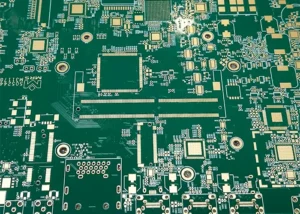
This stress causes the board to warp, making factors such as warpage and expansion-contraction ratios difficult to control, which in turn affects assembly and soldering, as shown in Figure 1.

For commercial products, designers must not only consider the performance factors mentioned above, but cost control is also of utmost importance.
Layer stacking strongly influences PCB performance and manufacturing cost. PCB engineers face a core challenge today.
They must develop stacking structures tailored to individual board requirements. These schemes need to balance electrical performance and cost simultaneously.
A Common 18-Layer Stackup
Stackup Overview
In high-speed PCB design, the 18-layer stackup shown in Table 1 is a commonly used stackup configuration.
This stackup offers several distinct advantages:
①The inner layers consist of 6 signal layers and 2 power layers, which can meet high-density routing requirements;
② All outer layers, the layers adjacent to the signal layers on both sides, and one side of the power layers feature a complete reference ground plane, fully meeting SI and PI requirements.
We set an appropriate distance between the signal layers and the reference plane. After impedance control, we maintain the line width within 0.1–0.15 mm.
This ensures routing density while complying with common PCB manufacturing standards such as the IPC series and QJ series;
③ The design uses core and prepreg (PP) of standard thicknesses, with a fully symmetrical laminate structure.
This facilitates material preparation for PCB manufacturers and simplifies the control of metrics such as board warpage and expansion-contraction ratios, thereby significantly ensuring product yield.
| Copper Layer / Dielectric Layer | Thickness |
|---|---|
| L1_TOP | 18 μm + 25–30 μm |
| PP | 0.09 mm |
| L2_GND1 | 18 μm |
| Core | 0.1 mm |
| L3_SIG1 | 18 μm |
| PP | 0.1524 mm |
| L4_GND2 | 18 μm |
| Core | 0.1 mm |
| L5_SIG2 | 18 μm |
| PP | 0.1524 mm |
| L6_GND3 | 18 μm |
| Core | 0.1 mm |
| L7_SIG3 | 18 μm |
| PP | 0.1524 mm |
| L8_GND4 | 18 μm |
| Core | 0.1 mm |
| L9_PWR1 | 70 μm |
| PP | 0.1524 mm |
| L10_PWR2 | 70 μm |
| Core | 0.1 mm |
| L11_GND5 | 18 μm |
| PP | 0.1524 mm |
| L12_SIG4 | 18 μm |
| Core | 0.1 mm |
| L13_GND6 | 18 μm |
| PP | 0.1524 mm |
| L14_SIG5 | 18 μm |
| Core | 0.1 mm |
| L15_GND7 | 18 μm |
| PP | 0.1524 mm |
| L16_SIG6 | 18 μm |
| Core | 0.1 mm |
| L17_GND8 | 18 μm |
| PP | 0.09 mm |
| L18_BOTTOM | 18 μm + 25–30 μm |
Table 1. Typical 18-Layer PCB Stackup
This stacking architecture offers great flexibility.
When the redesigned system adds substantial functions and brings routing difficulties, designers can insert one pair of signal and ground layers between L9 and L10.
This adjustment expands the stack to 20 layers. Alternatively, we can add two pairs of signal and ground layers symmetrically on both sides.
The stack then becomes 22 layers. These modifications do not impair the performance of original routing layers.
They also preserve the overall structural symmetry of the PCB.
Impedance Simulation
The design follows the QJ 831B standard. The standard specifies a minimum 0.09 mm dielectric spacing between adjacent copper foil layers.
It also requires an average copper plating thickness of no less than 25 μm for conductive circuit surfaces.
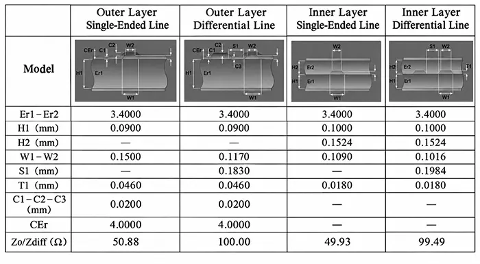
This study adopts SI9000 for impedance simulation. The simulation targets 50 Ω single-ended traces and 100 Ω differential pairs based on this stackup.
As shown in Table 2, the results fully meet the design requirements.
Designers can also fine-tune the stack spacing and trace widths according to specific PCB manufacturing standards to accommodate different design needs.
Issues and Improvement Goals
High-performance multilayer PCBs bring higher fabrication costs and longer lead times. Designers waste resources when they adopt these boards for high-pin, high-routing-density circuits without routing congestion.
PCB engineers confront a critical challenge. They reduce layer counts appropriately. They maintain strict control over signal integrity, power integrity, and board warpage at the same time.
Cost optimization remains another core objective. This work reduces layer numbers while balancing SI, PI and DFM performance.
We redesign the original 18-layer stackup into a 12-layer structure. The revised stackup still retains five inner signal layers and two inner power layers.
This arrangement meets the requirements of high-density routing.
Initial Reduction to 16 Layers
Proposed Solution
The 18-layer stack consists of 6 signal layers in the inner stack.
Reducing it to 16 layers requires only the removal of one adjacent pair of signal layers and a ground layer, as shown in Table 3.
| Copper Layer / Dielectric Layer | Thickness |
|---|---|
| L1_TOP | 18 μm + 25–30 μm |
| PP | 0.09 mm |
| L2_GND1 | 18 μm |
| Core | 0.1 mm |
| L3_SIG1 | 18 μm |
| PP | 0.1524 mm |
| L4_GND2 | 18 μm |
| Core | 0.1 mm |
| L5_SIG2 | 18 μm |
| PP | 0.1524 mm |
| L6_GND3 | 18 μm |
| Core | 0.1 mm |
| L7_SIG3 | 18 μm |
| PP | 0.1524 mm |
| L8_GND4 | 70 μm |
| Core | 0.1 mm |
| L9_PWR1 | 70 μm |
| PP | 0.1524 mm |
| L10_PWR2 | 70 μm |
| Core | 0.1 mm |
| L11_GND5 | 18 μm |
| PP | 0.1524 mm |
| L12_SIG4 | 18 μm |
| Core | 0.1 mm |
| L13_GND6 | 18 μm |
| PP | 0.1524 mm |
| L14_SIG5 | 18 μm |
| Core | 0.1 mm |
| L15_GND7 | 18 μm |
| PP | 0.09 mm |
| L16_BOTTOM | 18 μm + 25–30 μm |
Table 3. 16-Layer PCB Stackup Design
Feasibility Analysis
1. Consistency of Electrical Performance After Stackup Adjustment
This stackup follows the same logic as the 18-layer version. It provides full reference ground planes for every routing layer. Signal integrity and power integrity remain unaffected.
The spacing between signal layers and their corresponding reference planes remains unchanged. This arrangement eliminates rework on impedance and trace width configurations.
Engineers remove only one signal layer and shift a small set of dense routed traces to the component-free top layer.
2. Asymmetry Risk Caused by Different Copper Weights of Power Layers
However, it is worth noting that to meet power current capacity requirements, the copper thickness of the power layers is generally greater than that of the signal layers.
This means that after we adjust the stackup, we no longer place the power layers symmetrically at the board center to achieve overall stackup symmetry.
3. Symmetry Compensation Scheme and Production Verification
Here, adjusting the L8_GND4 layer—which is symmetrical to L9_PWR1—to have the same copper thickness as the power layer (using 70 μm for the power layer as an example) can significantly alleviate the board’s symmetry issues;
Although the L7_SIG3 layer, which is symmetrical to L10_PWR2, cannot be made thicker to meet impedance and manufacturing precision requirements, this stack-up is generally manageable in production.
Products using this design have entered mass production without any reported issues such as warpage or assembly and soldering problems.
Another Layer Reduction—14 Layers
Proposal of the Solution
To ensure the five signal layers and two power layers in the inner stack, any further reductions must be made to the ground layers, which makes it impossible to fully preserve the complete reference ground for all routing layers.
Since high-speed traces generally require at least two routing layers (e.g., separate TX and RX layers), the 14-layer design must retain two inner signal layers with dual reference grounds.
This design removes L4_GND2 and L8_GND4 from the 16-layer design; see Table 4 for the specific details.
| Copper Layer / Dielectric Layer | Thickness |
|---|---|
| L1_TOP | 18 μm + 25–30 μm |
| PP | 0.09 mm |
| L2_GND1 | 18 μm |
| Core | 0.1 mm |
| L3_SIG1 | 18 μm |
| PP | 0.1524 mm |
| L4_SIG2 | 18 μm |
| Core | 0.1 mm |
| L5_GND2 | 18 μm |
| PP | 0.1524 mm |
| L6_SIG3 | 18 μm |
| Core | 0.1 mm |
| L7_PWR1 | 70 μm |
| PP | 0.4064 mm |
| L8_PWR2 | 70 μm |
| Core | 0.1 mm |
| L9_GND3 | 18 μm |
| PP | 0.1524 mm |
| L10_SIG4 | 18 μm |
| Core | 0.1 mm |
| L11_GND4 | 18 μm |
| PP | 0.1524 mm |
| L12_SIG5 | 18 μm |
| Core | 0.1 mm |
| L13_GND5 | 18 μm |
| PP | 0.09 mm |
| L14_BOTTOM | 18 μm + 25–30 μm |
Table 4. 14-Layer PCB Stackup Design
Feasibility Analysis
In the above scheme, the two signal layers with dual reference grounds—L10_SIG4 and L12_SIG5—are retained, allowing for reliable routing of high-speed signals;
For low-speed I/O signals and DDR3/4, a single reference ground is fully sufficient to meet performance requirements.
Furthermore, this design restores symmetry to the stackup, making it more process-friendly for manufacturing compared to the 16-layer scheme.
The greatest challenge in this scheme actually lies with the power signals on L7_PWR1.
Since this layer has no adjacent ground planes to form a loop, it is at risk of PI issues due to factors such as electromagnetic noise interference.
To mitigate this problem as much as possible, we have significantly increased the spacing between L7_PWR1 and L8_PWR2 in the stack-up design to reduce mutual interference between different power supplies.
Designers should note the following when routing the board for this solution:
① Minimize routing on L6_SIG3 as much as possible;
Route only a small amount in congested areas such as the FPGA and DDR, and cover the rest of the board with a GND copper plane to provide as much reference ground as possible for the power signals on L7_PWR1;
② Place the core power signal planes on L8_PWR2; L7_PWR1 should only accommodate low-voltage, low-current digital power planes, with the remaining space on that layer filled with a GND network copper plane.
Final 12-Layer Design
Proposal of the Design
To further reduce the number of layers from the 14-layer design, we must remove two additional ground layers.
For the sake of simplicity, let’s assume the TOP side is the main component side;
If the BOTTOM side actually serves as the main component side, we can consider the design symmetrically.
This inevitably means that no signal layer can have dual reference grounds, so we must remove L11_GND4 from the 14-layer design.
The more difficult decision involves which of the other ground layers to keep:
① We cannot remove L13_GND5 because it serves as the only reference layer for the BOTTOM layer. The BOTTOM layer carries the routing of the 6th signal layer from the original 18-layer design;
② We cannot remove L9_GND3 either; otherwise, L8_PWR2 and L10_SIG4 would lose all reference grounds, which would severely degrade the PI and SI performance of those two layers;
③ L5_GND2 cannot be eliminated. Removing this plane would stack three signal layers in direct adjacency and degrade the signal integrity of critical signals, including DDR and CLK on the middle signal layer.
L2_GND1 therefore becomes the only viable layer for removal. Direct stacking of L1_TOP and L3_SIG1 is not allowed after deleting L2_GND1.
Designers insert L7_PWR1, a low-voltage and low-current digital power plane, between these two layers. L6_SIG3 originally references L7_PWR1.
Engineers move this signal layer along with the power plane to the new L3_SIG1 location. They increase the thickness of the new L11_GND3 layer to reduce stack asymmetry.
These adjustments produce the 12-layer stackup listed in Table 5.
| Copper Layer / Dielectric Layer | Thickness |
|---|---|
| L1_TOP | 18 μm + 25–30 μm |
| PP | 0.09 mm |
| L2_PWR1 | 70 μm |
| Core | 0.1 mm |
| L3_SIG1 | 18 μm |
| PP | 0.4064 mm |
| L4_SIG2 | 18 μm |
| Core | 0.1 mm |
| L5_GND1 | 18 μm |
| PP | 0.1524 mm |
| L6_SIG3 | 18 μm |
| Core | 0.1 mm |
| L7_PWR2 | 70 μm |
| PP | 0.1524 mm |
| L8_GND2 | 18 μm |
| Core | 0.1 mm |
| L9_SIG4 | 18 μm |
| PP | 0.4064 mm |
| L10_SIG5 | 18 μm |
| Core | 0.1 mm |
| L11_GND3 | 70 μm |
| PP | 0.09 mm |
| L12_BOTTOM | 18 μm + 25–30 μm |
Table 5. 12-Layer PCB Stackup Design
Feasibility Analysis
The above solution involves significant adjustments to the layer stacking, so we must note the following points in PCB design:
① The routing and copper fill for the new PWR1 layer must not only avoid sensitive circuit modules on the TOP layer—such as phase-locked loops and crystals—but also provide at least a complete power plane for the DDR signals on the new L3_SIG1 layer to serve as a reference;
We should then fill the remaining area of the layer with a GND copper plane;
② When we design the TOP layer, we may perform fan-out for the main components only at locations where power signals appear on PWR1, and then immediately drill a via to switch layers.
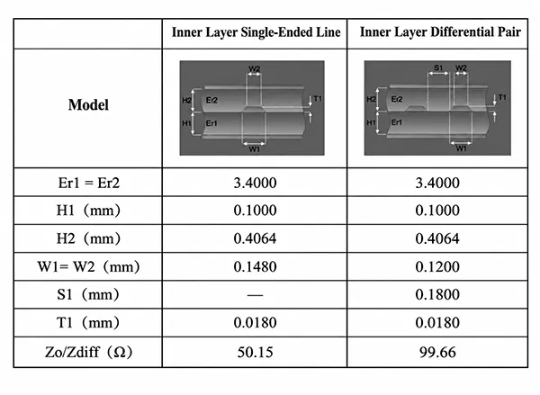
To minimize mutual interference between adjacent signal layers and ensure that a complete ground plane serves as the primary reference for the signals, this scheme increases the spacing between L3_SIG1 and L5_SIG2, L9_SIG4, and L10_SIG5 to 0.4064 mm.
We can adjust the specific distance based on actual SI and DFM requirements. According to the simulation results shown in Table 6, the impedance control in this design remains within acceptable limits;
However, since there is no complete reference plane above H2, the actual impedance may deviate from the values calculated by this model.
Although this approach increases the spacing between signal layers, crosstalk between signals remains a significant concern.
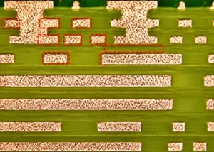
If we must route sensitive signals such as clocks or high-speed signals on adjacent signal layers, we should adopt zigzag routing patterns, as shown in Figure 2, to minimize crosstalk.
Even with this measure, we cannot completely resolve trace crosstalk. The design reserves five inner signal layers originally to handle boards with dense routing.
In such high-density digital regions, local ground planes or interlayer references are hard to arrange. This 12-layer stackup is therefore only applicable to circuits with moderate high-speed signal rates.

Contradictions in Low-Layer-Count Designs
A Common Low-Layer-Count Stackup
The stackup shown in Table 7 is a common 10-layer stackup design.
| Copper Layer / Dielectric Layer | Thickness |
|---|---|
| L1_TOP | 18 μm + 25–30 μm |
| PP | 0.09 mm |
| L2_GND1 | 18 μm |
| Core | 0.1 mm |
| L3_SIG1 | 18 μm |
| PP | 0.4064 mm |
| L4_SIG2 | 18 μm |
| Core | 0.1 mm |
| L5_GND1 | 70 μm |
| PP | 0.09 mm |
| L6_PWR1 | 70 μm |
| Core | 0.1 mm |
| L7_SIG3 | 18 μm |
| PP | 0.4064 mm |
| L8_SIG4 | 18 μm |
| Core | 0.1 mm |
| L9_GND3 | 18 μm |
| PP | 0.09 mm |
| L10_BOTTOM | 18 μm + 25–30 μm |
Table 7. Typical 10-Layer PCB Stackup
First, this stacking configuration is entirely feasible, and several products are already in mass production. Designers need to carefully manage routing and copper pour between L6_PWR1 and L7_SIG3.
For high-speed inner traces, local ground copper or cutouts are added on the neighboring signal layer. Figure 3 demonstrates this approach. It creates separate reference planes for each layer and meets signal integrity requirements.

Issues
Compared to the 12-layer design, this scheme omits one signal layer and one power layer. It cannot meet the requirement for five signal layers and two power layers in the inner layers, and it requires localized ground planes or interlayer references;
Therefore, it is not suitable for designs with high-speed, high-line-density layouts. Consequently, the 12-layer design is the minimum number of layers required for the research objectives of this paper.
Conclusion
In summary, there is no clear-cut superiority or inferiority among the stacking schemes described above.
PCB engineers must consider factors such as product reliability, cost, and manufacturing lead time comprehensively:
(1) An 18-layer full-configuration stackup is suitable for high-end products in fields with extremely high performance requirements, such as the military, satellite, and aerospace industries;
Where layout and routing density permit, this may be reduced to 16 layers as appropriate;
(2) A 12-layer stackup is suitable for designs with moderate high-speed signal rates, strict cost controls, and a requirement for five signal layers and two power layers on the inner layers;
Adjacent high-speed traces are staggered using a zigzag routing pattern to ensure performance;
(3) The 14-layer stackup strikes a balance between the two previous schemes. It cuts costs to a certain extent. It includes two inner signal layers: L10_SIG4 and L12_SIG5.
Each signal layer has two solid reference ground planes. This arrangement supports abundant high-speed signal routing.
This paper offers references for stackup planning of high-speed and high-density PCBs. Nevertheless, PCB design involves many other constraints.
These include enclosure fit, thermal performance and special fabrication processes. PCB engineers need to adjust the stack flexibly during design.