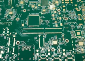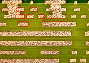
New energy vehicles with intelligent driving capabilities and artificial intelligence represent the most clearly defined growth areas in the current printed circuit board (PCB) market.
In recent years, the rapid development of vehicle electrification and intelligentization has accelerated the upgrade of automotive electrical and electronic architectures (EEA).
As core components of vehicle intelligence, various sensors and domain control units (DCUs) are entering a golden era of rapid growth.
According to QYResearch forecasts, we expect the global market for integrated cockpit-and-driving domain control units to reach a compound annual growth rate (CAGR) of 18.5% from 2025 to 2031;
We project that sales of mass-produced models with integrated cockpit-and-driving systems in China will rise 43% year-over-year in 2025, and we expect a CAGR of 36% from 2026 to 2030.
DCU serves as a core component for new-energy intelligent driving vehicles. Its reliability directly governs the safety of the intelligent driving system.
This imposes stricter requirements on data transmission speed and signal integrity of its supporting PCBs.
The author has carried out preliminary research on millimeter-wave radar PCB fabrication and the reliability of domain-control PCBs for intelligent vehicles.
Nevertheless, public literature is still lacking in three key areas: automotive-grade material selection for DCU PCBs, ultra-fine pitch BGA manufacturing, and corresponding reliability validation.
This study follows technology trends in cockpit and autonomous driving systems. It centers on automotive high-speed substrate selection for vehicle-grade applications.
The research covers tenting and modified semi-additive process (mSAP) fabrication. It also investigates local high-flatness control. Additional topics include the reliability of dense blind and buried vias and through-hole plating.
We also discuss the design and production of thick-copper, thin-dielectric structures. This work intends to offer practical guidance for the PCB manufacturing sector.
Evolution of Domain Control Technology in Smart Vehicles
-
EEA Evolution and Integration with Intelligent Driving
EEA evolves gradually through three stages. It starts from traditional distributed electronic control units (ECUs).
Then it transitions to domain-centered architectures. Finally, it develops into a centralized computing architecture.
We divide intelligent vehicles into five classic functional domains: powertrain, chassis, body, cockpit and autonomous driving.
The powertrain domain manages propulsion systems. It covers engines, batteries and power distribution.
The chassis domain governs vehicle driving dynamics. It handles braking, transmission and steering functions.
The cockpit domain runs in-vehicle electronic information systems. Typical units include infotainment, central control and instrument panels.
The body domain controls body-related electrical features. It manages lamps, windows and gateway communication.
The autonomous driving domain executes self-driving functions. It processes data across perception, decision and control layers.
The characteristics and quality control requirements of the corresponding domain-control PCBs vary accordingly.
① Currently, there are three major trends in domain control technology development among mainstream automakers:
The centralization trend, represented by the powertrain domain, which involves further consolidating the powertrain, chassis, and body domains into a single vehicle-wide domain;
② The autonomous driving domain represents this convergence trend.
The autonomous driving and cockpit domains are critical for vehicle modernization, intelligence and personalization.
They evolve along the path of cockpit-driving convergence, as shown in Table 1.
③ The trend toward centralized computing for domain control, which involves the development of cockpit-driving integration and centralized computing to reduce costs and share computing power.
It is projected that by 2027, the penetration rate of the Central Control Unit (CCU) architecture in new vehicles will exceed 30%.
| Stage | Integration Approach | Technology Roadmap |
|---|---|---|
| Cockpit-Driving Separation | Two-Box Stage (two boxes/two boards) | The cockpit domain and intelligent driving domain operate independently. |
| Cockpit-Driving Integration 1.0 | Multi-Board Stage (multi-board, one box/two boards) | Functions are distributed across independent PCBs and communicate via Ethernet (100–1,000 Mb/s). |
| Cockpit-Driving Integration 2.0 | Single-Board Stage (one board, one box/one board) | Multiple system-on-chip (SoC) devices are integrated onto a single PCB and interconnected via PCIe (16 GT/s). |
| Cockpit-Driving Integration 3.0 | Single-Chip Stage (one chip) | Functions are highly integrated and run on a single SoC. |
Table 1. Evolution of Different Cockpit-Driving Integration Technologies
-
Typical Design Solutions for the Cockpit Domain and Intelligent Driving Domain
Single-board, single-chip integrated cockpit and driving domain controllers depend on higher computing performance from high-grade automotive chips.
DCUs for different levels of autonomous driving have different computing power requirements.
DCUs for Level 2 autonomous operation require 10–30 TOPS. Level 3 DCUs support 30–100 TOPS of computing capacity.
Level 4 DCUs call for 200–500 TOPS. Designers expect Level 5 systems to deliver over 1,000 TOPS.
Cockpit domain chips with CPU performance ≥600 kDMIPS have entered initial mass application.
DMIPS stands for Dhrystone million instructions per second. TOPS stands for tera operations per second.
SoCs need to process growing volumes of data. DCU PCB designs are gradually shifting from conventional multilayer through-hole boards (MLB) to high-density interconnect (HDI) structures.
Mainboards are typically 1st- or 2nd-order HDI, while module boards can reach up to 5th or even 6th order;
We have designed their BGA (ball grid array) pitch down to a minimum of 0.35 mm, and designers already use this solution.
Specific design elements for each generation of Qualcomm’s cockpit-domain, autonomous-driving-domain, and integrated cockpit-and-driving SoCs are shown in Table 2.
| No. | Domain Controller | SoC Platform | PCB Stackup | Outer Layer Trace Width/Spacing (μm) | Inner Layer Trace Width/Spacing (μm) | BGA Pitch (mm) |
|---|---|---|---|---|---|---|
| 1 | Cockpit Domain | 820A | HDI 1+6+1 | 100/127 | 75/75 | 0.65 |
| 2 | Cockpit Domain | 8155 | HDI 3+4+3 | 100/100 | 75/75 | 0.70 |
| 3 | Cockpit Domain | 8195 | HDI 5+2+5 | 75/75 | 50/50 | 0.40 |
| 4 | Cockpit Domain | 8295 | MLB 10–12L | 90/115 | 90/100 | 0.60 |
| 5 | Cockpit Domain | 8255 | HDI 2+4+2 | 100/100 | 80/100 | 0.60 |
| 6 | Intelligent Driving Domain | 8397 | HDI 1+10+1 | 80/100 | 75/90 | 1.00 |
| 7 | Intelligent Driving Domain | 8620 | HDI 2+4+2 | 76/100 | 60/90 | 0.65 |
| 8 | Intelligent Driving Domain | 8650 | HDI 5+2+5 | 76/120 | 50/100 | 0.80 |
| 9 | Intelligent Driving Domain | 8797 | HDI 1+10+1 | 100/130 | 60/100 | 1.00 |
| 10 | Integrated Cockpit-Driving Domain | 8775 | HDI 2+8+2 | 75/100 | 60/100 | 0.65 |
Table 2. Overview of Domain Controller PCB Design Requirements for Qualcomm Automotive-Grade SoC Platforms
Signal Integrity Control for DCU PCBs
As a core component in vehicles, the reliability of materials selected for high-tier HDI PCBs is a primary concern.
The high-computing integrated cockpit-and-driving DCU functions essentially as an on-board high-performance computer (HPC).
Its signal integrity (SI) becomes a critical bottleneck that restricts further system performance gains.
-
High-Speed Transmission Requirements and Material Selection for Automotive-Grade High-Speed Applications
1. Background of PCIe 5.0 High-Speed Evolution for Automotive DCU
To meet the demands of Level 3 and higher advanced driver-assistance systems (ADAS), high-speed data transmission in the DCU is upgrading from PCIe 4.0 to PCIe 5.0.
Signal traces on DCU PCBs are shorter than those found in data center servers.
Even so, insertion loss specifications grow tighter. PCB stacking and structural designs also become more intricate.
The design considerations for domain controller PCBs across different ADAS levels are shown in Table 3.
2. Key Selection Indicators for Automotive High-Speed Dielectrics
Given cost, signal integrity (SI), manufacturability, and reliability requirements, the selection of automotive-grade high-speed materials is critical.
We focus on the following key considerations: Glass transition temperature (Tg) and coefficient of thermal expansion (CTE), which strongly affect multiple lamination cycles;
Dielectric constant and loss factor (Dk/Df), which directly influence SI;
Halogen-free properties and high tracking index (CTI), which relate to conductive anode filament (CAF) performance.
The following section presents reliability and SI tests conducted on four typical automotive-grade materials of different grades selected from the industry (see Table 4).
| Intelligent Driving Level | Interface Technology | Data Transfer Rate (Gbps) | Insertion Loss Requirement | Main HDI Stackup | Application Scenarios and SoC Configuration |
|---|---|---|---|---|---|
| L2–L3 | PCIe 3.0 | 8 | −0.65 dB/in @ 4 GHz | 1+8+1, 2+6+2, 3+4+3, 5+2+5 | Cockpit domain and intelligent driving domain; primarily single-board, single-chip configurations |
| L2–L4 | PCIe 4.0 | 16 | −0.85 dB/in @ 8 GHz | 2+6+2, 2+8+2, 3+10+3, 5+2+5 | Advanced intelligent driving and cockpit-driving integration; single-board single-chip and dual-chip configurations |
| L3–L4 | PCIe 5.0 | 32 | −0.96 dB/in @ 16 GHz | 2+8+2, 2+10+2, 3+8+3, 3+12+3 | Cockpit-driving integration and autonomous driving; single-board dual-chip and quad-chip configurations |
| L4–L5 | PCIe 6.0 | 64 | −1.79 dB/in @ 28 GHz | 3+12+3, 4+8+4 | Central Computing Unit (CCU) and autonomous driving |
Table 3. PCB Design Requirements for Domain Controllers at Different Levels of Intelligent Driving
| No. | Material | High-Speed Grade | Halogen-Free | Copper Foil Type | Tg (°C, DMA) | Z-CTE (%) (50–260 °C) | X/Y-CTE (×10⁻⁶/°C) | Dk/Df (10 GHz) | Storage Modulus (GPa) (250 °C) |
|---|---|---|---|---|---|---|---|---|---|
| 1 | A | M2 Grade | Yes | RTF | 210 | 1.8 | 11–13 | 3.8/0.019 | 4.3 |
| 2 | B | M4 Grade | Yes | RTF2 | 280 | 1.3 | 9–10 | 3.4/0.008 | 11.5 |
| 3 | C | M6 Grade | Yes | HVLP | 290 | 1.4 | 9–10 | 3.5/0.005 | 10.0 |
| 4 | D | M7 Grade | Yes | HVLP | 200 | 1.8 | 9–10 | 3.2/0.004 | 5.5 |
Table 4. Comparison of Technical Parameters of Different Grades of Automotive-Grade Low-Loss PCB Materials
Note: RTF stands for “reverse treated foil,” and HVLP stands for “hyper very low profile” copper foil; A, B, C, and D are the codes for the corresponding types of copper-clad laminate substrates.
3. Thermal and CAF Reliability Test Setup and Results
All four materials adopt the same 4+4+4 HDI stackup. They complete a thermal reliability test comprising 20 lead-free reflow cycles at a peak temperature of 260 °C (Figure 1).
Every sample uses a 300 μm wall-to-wall spacing for blind vias. Blind vias maintain a 330 μm clearance from buried vias.
Buried vias sit 100 μm away from copper edges. Inner-layer traces follow a line width/spacing specification of 63.5 μm / 89 μm.
All materials meet the requirements of this combined test sequence.
They withstand three lead-free reflow cycles at a peak temperature of 260 °C.
Samples receive preconditioning at 85 °C and 85% RH for 96 h.
They finish 1000 h of CAF testing under 85 °C, 85% RH and 100 V bias while keeping resistance above 10⁸ Ω.
4. Insertion Loss Comparison for 28 GHz High-Speed Signals
An 85 Ω ± 10% ribbon with a line width/spacing of 115/190 μm was selected for comparative testing of the corresponding insertion loss, as shown in Figure 2.
As shown in Figure 2, only Class C and Class D automotive-grade low-loss materials can meet the high-speed domain control requirement of ≤1.79 dB/inch at 28 GHz.


-
Fine-Line Fabrication and Characteristic Impedance Control
The BGA pitch and fine-line width/spacing designs for high-order HDI DCU products are trending downward.
In the 4+2+4 HDI cockpit domain, 0.35 mm pitch BGA differential lines with a line width/spacing of 38/40 μm, laser via diameters/ substrates with ϕ75 μm/ϕ155 μm, and in-board differential impedance control (75±5%) Ω.
The design adopts laser direct imaging (LDI) for field partitioning.
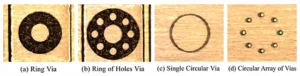
It uses an annular dot-matrix target for laser blind vias instead of a standalone copper pad target.
Figure 3 shows this structure. This method effectively addresses alignment errors from repeated lamination and laser drilling in high-order HDI boards.
It supports stable mass production of laser vias with a 40 μm single-sided landing pad.
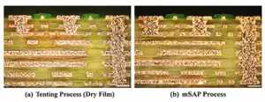
At the same time, 3 μm low-roughness copper foil was used for the initial plating layer, and comparisons were made with the tenting and mSAP processes, which aim to achieve a final copper thickness of (18±3) μm.
Test results demonstrate the following performance. We adopt precise linewidth compensation and optimized vacuum two-fluid etching for the tenting process.
The etched linewidth falls between 38.76 μm and 42.31 μm. Its process capability index Cpk reaches 1.36, and the etching factor is 8.6.
The impedance control range is 5.39 Ω, with a Cpk of 1.26.
For the mSAP process, we control the linewidth from 36.24 μm to 38.98 μm.
It achieves a Cpk of 1.69 and an etching factor of 19.9. The impedance control range is 4.41 Ω·μm, with a Cpk of 1.45.
It can be seen that the reduction etching method is comparable to the mSAP process, as shown in Figure 4.
DCU PCB Manufacturing Process and Quality Control
-
Board Warpage and High Flatness Control
DCU module board manufacturing involves multiple assembly steps.
To improve the reliability of fine-pitch, large-size BGA surface-mount components (such as preventing solder cracking), there is a growing demand for BGA areas with flatness requirements of ≤100 μm or even ≤80 μm.
Comparative testing was conducted using the shadow moiré method.
Figure 5 shows the flatness performance of PCBs with corresponding laminate designs for the four automotive-grade low-loss materials listed in Table 4 at temperatures ranging from 30 to 260 °C.
The local flatness of the 80 mm × 80 mm BGA area, from lowest to highest, is B < C < A < D, indicating that the higher the storage modulus, the higher the Tg, and the lower the Z-CTE, the more favorable the conditions are for flatness control.
However, for automotive-grade M7 laminate type D, poor resin flow, a high filler content, and the inability to fully release internal stress during lamination resulted in relatively poor flatness.

Designers choose low-resin-content semi-prepregs for symmetrical stackups.
The relative residual copper variation between layers is controlled within ≤5%.
Engineers reserve copper-clad processing margins along panel edges.
Several manufacturing adjustments support stable production.
Operators prolong lamination holding time to ensure sufficient resin crosslinking.
A longer cooling phase helps release residual thermal stress.
Tg-point baking after mechanical drilling and skip drilling further relieve mechanical stress.
These measures are applied to the 2+6+2 HDI stack DCU on Board A in Table 4.
Shadow Moiré analysis continuously monitors its BGA flatness across the full temperature range of 30–260 °C.
The improvement was significant, with flatness deviation decreasing from 109.2 μm to ≤60 μm, with overall board warpage ≤0.3%, as shown in Figure 6.

-
Reliability of High-Density Buried and Blind Vias
1. Limitations of POFV+VOI Design for DCU Boards
As discussed earlier in this article, it is not advisable to use the “Plug-Over-Fill-Vias” (POFV) + “Via on IVH” (VOI) design for domain-controlled boards.
Domain controller boards adopt dense buried via layouts. Some samples still fail reliability tests, including 20 cycles of lead-free reflow.
Engineers have tried multiple improvement measures. These measures include slowing the browning rate and adding post-browning drying.
They also apply chemical etching or plasma etching on the resin layer above buried vias.
These treatments aim to lower internal board stress. The final goal is to enable the board to pass the 20-cycle lead-free reflow reliability test.
2. T288 Performance and Delamination Risk of Buried-Via HDI
For example, a 3+10+3 HDI structure DCU main board with buried via wall spacings ≤0.3 mm and local via densities exceeding 50 vias experienced board delamination.
We conducted a comparative test on two high-Tg, halogen-free, low-Dk boards with very similar technical specifications.
After multiple lamination cycles, we observed significant differences in the measured Tg, Z-CTE, and especially the T288 values (see Table 5).
Halogen-free PCBs commonly adopt DOPO-based flame retardant systems.
Boards with this formula tend to suffer resin degradation and embrittlement.
Their resistance to delamination drops sharply after repeated high-temperature lamination.
T288 performance relies heavily on the resin’s cohesive strength and Z-axis bonding strength under high temperature.
This property strongly determines the thermal resistance and reliability of such PCBs.
For example, the probability of an “E” failure under T288 was 46.5% for Board A, while Board F achieved a 100% pass rate.
Therefore, when designing HDI boards, close attention must be paid to the T288 performance of the actual laminated assemblies.
| PCB Material | Dk/Df (10 GHz) | Tg (°C, TMA) – Copper-Clad Laminate Specification | Z-CTE (×10⁻⁶/°C), α1/α2 – Copper-Clad Laminate Specification | T288 (min) – Copper-Clad Laminate Specification | Tg (°C, TMA) – Measured 3+10+3 Stackup PCB | Z-CTE (×10⁻⁶/°C), α1/α2 – Measured 3+10+3 Stackup PCB | T288 (min) – Measured 3+10+3 Stackup PCB |
|---|---|---|---|---|---|---|---|
| E | 3.5/0.010 | 160.0 | 37/170 | >60 | 149.1 | 55/330 | 0 |
| F | 3.59/0.009 | 165.0 | 35/180 | >60 | 159.1 | 35/245 | 11.43 |
Table 5. Comparison of Key Technical Parameters of Two High-Tg Halogen-Free Laminates and Their Multilayer PCBs
3. Interfacial Failure Mechanism of Dense Blind Vias with RTF Copper Foil
Domain controller boards feature dense blind via layouts, with via wall spacing down to 100 μm or less.
This design targets better signal integrity and supports fine-line fabrication.
When laminating HDI boards with RTF copper foil and high-speed substrates, the bond between RTF foil and high-speed resin is relatively weak.
Dense CO₂ laser drilling creates sharp local temperature spikes.
Temperature rises beyond the resin glass transition temperature (Tg). The resin softens and expands along the Z-axis.
This effect triggers micro-blasting at the RTF copper-resin interface in dense blind via zones.
Local delamination of the RTF copper also occurs. These defects lead to failures in the subsequent electroless copper plating process.
4. Optimization Countermeasures for Laser Drilling and Lamination
Several countermeasures relieve these issues effectively. Manufacturers adopt high-adhesion RTF copper grades.
Prepregs undergo vacuum dehumidification before lamination. CO₂ laser parameters are tuned to cut heat buildup.
Adjustments include reduced single-pulse energy, higher pulse frequency, smaller spot overlap, and optimized scanning paths.
-
Control and Improvement of Coating Cracks
1. TCT Acceptance Criteria for DCU Boards
New energy vehicle DCU boards have strict thermal cycle test (TCT) specifications.
Their resistance change after TCT must not exceed 5%. No corner or hole-wall coating cracks are allowed.
Any hole-wall crack shall cover no more than 10% of the copper thickness.
2. Root Factors of Plating Cracking in TCT
Coating cracking during TCT is linked to multiple factors.
These include the board’s Z-axis CTE, curing degree of lamination resin, and residual stress released after lamination.
It also relates to drying after drilling and plating, coating crystallization from electroplating, and total organic carbon (TOC).
3. Laminate Material Effect on PTH Corner Cracking
During TCT testing of the HDI 3+10+3 DCU main board at −40 to 140 °C over 1,500 cycles, 5% of the plating on both buried vias and through-hole corners failed due to cracking.
This failure could not be mitigated by stress relief (lamination, drilling, and post-plating baking), stress relief (lamination, drilling, and plating drying), or thickening treatment via DC plating in fresh plating solutions;
However, after replacing Board E with Board F (see Table 5), parallel comparison tests showed that Board E exhibited corner cracking after 900 cycles and a resistance change rate exceeding 10%, whereas Board F withstood 1,500 cycles without any cracking.
This demonstrates that laminates with higher Tg and lower Z-CTE can significantly reduce corner coating cracks in DCU HDI through-holes (PTHs).
4. Influence of Plating Solution TOC on TCT Crack Resistance
A comparative test of the PTH copper TCT for an HDI 2+6+2 DCU main board at -40 to 160 °C over 1,000 cycles was conducted as follows:
The same halogen-free laminate with a high Tg (TMA 170 °C) was laminated and subjected to direct current vertical continuous plating (VCP) at the same current density;
However, different plating qualities were obtained in different life-test solutions.
For example, under condition a, the flash plating TOC was 1,072, the VCP TOC was 2,300, while under Condition B, the values were 711 and 926, respectively.
The results showed that in Condition A, coating cracks appeared in the TCT as early as 800 cycles, with the maximum crack length reaching 9.2% of the perforated copper thickness;
By 1,000 cycles, the condition had deteriorated further to 15.7%, although the rate of change in resistance remained within the ±5% requirement;
However, no cracks appeared in the plating solution under Condition B even after 1,000 TCT cycles, and the resistance change rate remained within ±5%.
It can thus be seen that as the TOC of the plating solution increases, the content of organic impurities in the plating layer rises, which reduces the overall strength of the copper-filled via and consequently degrades the crack resistance of the TCT plating layer.
Therefore, strict control of the plating solution’s TOC is required for high-reliability DCU boards.
-
Thick Copper, Thin Dielectric, Thick CAF Reliability
1. Design Purpose of Thick Copper Power/Ground Layers for High-Power DCU
As SoC computing power increases, power consumption rises and transient currents grow; thick copper power and ground layers serve as heat dissipation planes and improve thermal management.
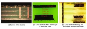
For example, the NVIDIA Thor-U integrated cockpit and driver DCU2+6+2 HDI board requires an inner layer copper base thickness of 70 μm (2 oz), as shown in Figure 7(a).
This design aims to lower loop inductance and improve the low-frequency impedance of the power distribution network (PDN). It also controls the overall board thickness.
The dielectric between the thick copper power plane and its neighboring ground plane is specified at ≤0.100 mm, with 0.080 mm as the typical value.
A representative stack uses two pieces of 1037 prepreg with 75% resin content. 35 μm and 70 μm copper foils are arranged on the top and bottom sides of this dielectric structure, respectively.
2. Resin-Filling Deviation Between Asymmetric Copper Thicknesses
Theoretical lamination model calculations indicate that the resin filling is relatively sufficient, with no risk of lamination voids;
As shown in the cross-sectional inspection of the actual laminated board in Figure 7(b).
Figure 7(b) illustrates this phenomenon. The 1037 flat glass fabric features fine mesh and low permeability.
The 70 μm circuit needs a large amount of resin for filling.
Yet resin supply is limited to one side only. On the 70 μm copper side, the average resin thickness reaches merely 5.70 μm, with a minimum value of 3.15 μm.
By contrast, the 35 μm copper side has an average resin thickness of 11.40 μm and a minimum of 9.25 μm. Table 6 summarizes these data.
3. CAF Failure Risk and Optimized Prepreg Stackup Scheme
Due to the actual thinness of the resin layer, the 70 μm copper-side layer is highly prone to CAF failure, as shown in Figure 7 (c).
Improvement tests indicate that this issue can be effectively resolved by using a stackup design consisting of two 1,037/RC79% sheets with a higher resin content or two 1,080/RC69% sheets with better permeability.
Conclusion
In recent years, the rapid growth of the new energy and autonomous vehicle market has brought new opportunities and challenges to the development of high-end domain-controlled PCBs.
Among these, the cockpit-and-driving-integrated DCU PCB—which features high computing power, high current capacity, and superior heat dissipation—is a typical example of a high-tier, high-performance, and high-value HDI product.
This paper systematically reviews the technological evolution of DCUs and their typical PCB design features.
It shows that M6-grade and above automotive high-speed materials support the signal integrity requirements of high-speed domain controllers.
These materials achieve a loss performance of ≤1.79 dB/inch at 28 GHz.
At the process level, this paper verifies the equivalence of the tenting method and the mSAP process in the fabrication of high-density HDI boards featuring 0.35 mm pitch BGA with two-wire penetration.
At the performance level, through optimized design and process control, a breakthrough was achieved with a surface roughness of ≤60 μm across the entire temperature range of 30–260 °C;
We conducted an in-depth analysis of the causes and countermeasures for delamination and plating cracks in high-density buried/blind via PCBs;
And established a CAF reliability design model for PCBs with thick copper and thin dielectric layers.
The key technologies and implementation pathways proposed in this study can serve as a reference for related industries.