Large-model training, distributed computing clusters, and high-speed computing hardware are developing rapidly.
Core hardware, including AI servers, GPU accelerator cards, and computing switches, imposes stringent requirements on PCBs.
The key demands cover high-speed signal transmission, power integrity, and long-term reliability. Traditional multilayer PCB via structures introduce the inherent stub effect.
This effect triggers multiple signal defects for ultra-high-speed interconnects. Typical scenarios include 112/224 Gbit/s PAM4 links, PCIe 5.0/6.0 and NVLink interfaces.
The induced problems involve signal attenuation, resonant crosstalk, elevated bit error rates, and degraded computing performance. Becoming a core bottleneck that limits the efficient unleashing of AI computing power.
Currently, the processing speeds of digital devices are continuously accelerating, and signal frequencies are rising accordingly.
Published research reveals multiple influencing factors for signal integrity. These factors include PCB layout, substrate materials, transmission traces, connectors, and chip packaging.
Among them, through vias stand out as a critical contributor. Standard through vias create severe interference for high-speed signal propagation.
Back-drilling is a secondary drilling operation applied to plated through vias. It removes redundant copper on the hole barrel. This shortens the stub length of the via. This suppresses the capacitive parasitic effect.
The process improves high-speed signal transmission and raises the data bandwidth of high-speed connectors.
Among various back-drilling processes, back-drilling of microvias in ball grid array (BGA) packages presents the greatest challenge.
Due to layout space constraints, the via diameters in BGA areas are extremely small;
Conventional vias adopt diameters of merely 0.25 mm or 0.30 mm, and the corresponding back-drill diameters need to be controlled between 0.45 mm and 0.55 mm.
This process imposes stringent requirements on depth control accuracy, hole positioning accuracy, and surface finish quality.
Among these, the issues of burrs and blocked holes resulting from back drilling remain persistent technical challenges facing the industry.
Major Existing Issues
Stubs are a core defect that limits the performance of high-speed PCBs.
On high-speed PCBs, stubs generate parasitic capacitance and inductance under high-frequency signals of 10 Gbit/s or higher, leading to impedance discontinuities and compromising signal integrity.
The impact becomes more significant as data rates and the number of layers increase;
Therefore, back-drilling is mandatory for stubs exceeding 0.25 mm, and AI 112/224 Gbit/s link specifications impose even stricter requirements.
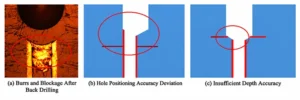
Currently, the back-drilling of microvia holes primarily faces the following issues (as shown in Figure 1):
(1) Burrs and Clogged Holes after Back-drilling
Back-drilling leaves the copper layers at intersection points suspended, which generates burrs. Meanwhile, the tiny microvia diameter provides limited space for chip evacuation.
This issue becomes more severe when small through-holes are combined with microvia back-drilling.
(2) Deviations in Back-drilled Hole Positioning Accuracy
Since back-drilling of microvias is a secondary drilling process, and given the narrow diameter of the microvias, hole positioning deviations are prone to occur during machining.
(3) Insufficient Back-drilling Depth Accuracy
Microvias feature tiny hole diameters. This characteristic increases the difficulty of depth control for drilling equipment. As a result, it is hard to satisfy the precision tolerance requirements for back-drilling depth.
This study focuses on analyzing and experimentally verifying the issues of burrs and clogged holes in the back-drilling of BGA microvias.
Experimental Section
Analysis of Causes
The most fundamental difference between micro-hole back drills and standard back drills lies in the smaller bore diameter of micro-hole back drills, which is also the root cause of frequent clogging and burr formation:
(1) The back-drill bit has a small bore diameter, which limits the space inside chip flutes and greatly weakens chip removal capability.
(2) Drilling small-diameter holes subjects the drill to uneven stress, making it prone to burr formation;
At the same time, poor dust extraction leads to dust accumulation and subsequent hole blockage;
(3) Insufficient alignment accuracy between the blind hole and the through-hole exacerbates burrs and hole blockage defects;
(4) Under conventional processes, the copper thickness in through-holes can reach 15 μm or more;
Completely cutting through the copper in small-hole structures is extremely difficult.
Evaluation Tests
There are currently two standard back-drilling processes.
Process 1: Inner layers → Laminating → Drilling → Electroless copper plating/Electroplating → Outer layer patterning → Back drilling → Automated Optical Inspection (AOI) → Wet film → Subsequent standard processes.
Process 2: Inner layer → Lamination → Drilling → Copper plating/Electroplating → Pattern plating → Tin plating → Back drilling → Development/Alkaline etching → AOI → Wet film → Subsequent standard processes.
When Process 1 is adopted for microvia back-drilling, heavy internal burrs and hole blockage occur. These defects halt normal production.
Process 2 includes an additional etching step, resulting in better quality than Process 1;
However, fine holes are prone to clogging due to dust, preventing the etching process from removing burrs, and the defect rates for burrs and clogged holes remain relatively high.
Small diameter holes inherently make chip evacuation difficult. One feasible solution reduces cutting resistance.
We can thin the copper layer of through vias. This eases back-drilling cutting loads and improves machining quality.
Researchers designed a novel experimental process based on this strategy: inner layer fabrication → lamination → drilling → primary plating → back drilling → secondary plating → outer layer patterning → follow-up standard procedures.
We precisely tune the copper thickness of through vias in the primary plating step. This lowers the cutting difficulty of back-drilling.
Combined with follow-up process operations, the approach fully eliminates burr formation and hole clogging during microvia back-drilling.
The test parameters for back-drilling are shown in Table 1.
| Through-Hole Diameter | Back Drill Diameter | Back Drill Width | Back Drill Depth |
|---|---|---|---|
| 0.25 | 0.45 | 0.65 | 0.5, 1.0, 1.7 |
| 0.30 | 0.50 | 0.80 | 0.5, 1.0, 1.7 |
Table 1. Back Drilling Test Parameters (Unit: mm)
Test Results and Analysis
1. Through-Hole Position Accuracy Testing
Operators adopted a hole-position accuracy scanner for full inspection of all through-holes and assessed the positional accuracy control of holes produced in a single drilling run.
The results of the through-hole drilling position accuracy inspection are shown in Table 2.
As shown in Table 2, the hole position accuracy for the 0.25 mm and 0.30 mm through-holes was excellent, with a maximum deviation of only 50 μm and a process capability index (Cpk) value well above 1.33.
| Sample No. | Maximum Deviation (μm) – 0.25 mm | Maximum Deviation (μm) – 0.30 mm | Cpk – 0.25 mm | Cpk – 0.30 mm |
|---|---|---|---|---|
| 1 | 25 | 50 | 4.41 | 4.07 |
| 2 | 50 | 50 | 4.10 | 3.44 |
Table 2. Positional Accuracy of Through-Hole Drilling
2. Accuracy Testing of Back-Drilled Hole Alignment with Through Holes
Researchers carried out cross-sectional analysis with a metallographic microscope.
They collected no fewer than 30 samples for each test condition to assess the positional precision control of back-drilled holes.
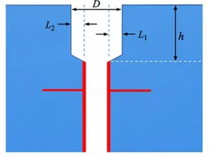
The back-drilled hole accuracy deviation was calculated as (L1 − L2)/2 (where L1 and L2 are the unilateral safety margins on either side of the back-drilled hole), as shown in Figure 2. where D is the back-drilled hole diameter and h is the back-drilling depth.
Based on the Cpk test data for the alignment accuracy between the back-drilled hole and the through-hole, the alignment deviation for 0.45 mm and 0.50 mm back-drilled holes relative to the through-hole is ≤0.10 mm, with a Cpk ≥ 1.33, indicating that the accuracy meets the specified requirements.
3. Analysis of Factors Affecting Alignment
Researchers conducted an analysis of variance for the two back-drill diameters of 0.45 mm and 0.50 mm.
The results showed that P > 0.05, indicating no significant difference in back-drill alignment accuracy between the two diameters.
Researchers performed an analysis of variance for the three back-drill depths: 0.5 mm, 1.0 mm and 1.7 mm. The results showed that P > 0.05, indicating that back-drill depth does not significantly affect hole alignment accuracy.
Researchers performed an analysis of variance for the two BGA pitch values of 0.65 mm and 1.0 mm. The results showed that P > 0.05, indicating no significant correlation between pitch and back-drilling alignment accuracy.
The above ANOVA results show that back-drill diameter, depth, and BGA pitch exert no significant influence on back-drilling alignment accuracy.
Instead, drilling parameters and process approaches dominate this accuracy metric.
4. Burrs and Hole Blockage Defects
Inspectors examined all sample boards via visual examination and backlight checking with a 10× magnifier.
A design of experiments (DOE) was established to statistically analyze the hole blockage rate and burr defect rate after back-drilling.
The experimental design selected the following drilling parameters: rotational speed (S): 65,000, 100,000, 140,000, and 167,000 r/s; feed rate (F):
10, 22, 36 mm/min; and retraction speed (U): 258, 337, 416 mm/min.
The results indicate a hole blockage rate of 0–0.5% under the conditions: spindle speed S = 65000 r/s, feed rate F = 36 mm/min, retraction speed U = 337 mm/min.
Using these parameters to fabricate different board models, the test results are shown in Table 3. The optimized drilling parameters achieve a zero plugging rate for back drilling;
The combinations of 0.25 mm through-holes paired with 0.45 mm back drills and 0.30 mm through-holes paired with 0.50 mm back drills resulted in no burrs or plugging defects after machining.
| Production Batch No. | Quantity (pcs) | Number of Damaged Holes | Total Number of Holes | Hole Damage Rate (%) |
|---|---|---|---|---|
| A1 | 11 | 0 | 18,788 | 0 |
| A2 | 60 | 0 | 13,320 | 0 |
| A3 | 48 | 0 | 27,648 | 0 |
| A4 | 34 | 0 | 63,104 | 0 |
Table 3. Test Results After Parameter Optimization
5. Reliability Testing
Using a reflow soldering machine, the test conditions were set as follows: temperature of 217 °C or higher for 120–150 seconds;
Peak temperature of 260 °C; dwell time of 20–30 seconds at 255 °C or higher; and a total of five reflow soldering tests.
Researchers observed no delamination on the hole walls from the test results, so the test met acceptance requirements.
Conclusion
This paper presents a systematic study of the entire microhole back-drilling process.
The results indicate that, aside from the inherent effects of hole diameter, the alignment accuracy between the back-drilled hole and the through-hole is the key factor causing burrs and clogging within the hole.
By optimizing the microhole back-drilling process and machining methods, and through experimental testing to determine the optimal parameter combination, this study has completely resolved the issues of burrs and clogging in microhole back-drilling.
Both process stability and product reliability meet the requirements for mass production.