
A couple of days ago, I designed a power board, but because the trace width was too narrow, one of the traces burned out the moment power was applied.
To solve this problem, we ultimately had to replace the burned-out trace with an external jumper.
The PCBs used at my previous company were typically 6-, 8-, or 10-layer boards, with components arranged very densely, leaving very little space.
Therefore, to accommodate thicker traces, we usually had to continuously compress the available space during layout.
However, sometimes there simply wasn’t enough space, and due to layout constraints, we had no choice but to appropriately reduce the trace width as needed to complete the routing.
Based on past experience, we’ve determined that, under normal circumstances, a 1-ampere current generally requires a 1-millimeter-wide trace to be sufficient.
So, based on this experience, can we infer that a current of 10 amperes would require a 10-millimeter-wide trace?
When a PCB provides ample space, designers can indeed design trace widths according to this ratio.
However, in multilayer PCBs where space is limited, designers may not be able to use a 10-millimeter trace width.
This is because multilayer PCBs typically have very limited internal routing space, and wider traces occupy more area, potentially preventing designers from accommodating thicker traces.
Therefore, for high-current applications, selecting an appropriate trace width requires a comprehensive consideration of multiple factors, including current load, trace cross-sectional area, heat dissipation requirements, and space constraints.
Making the best design decisions requires a certain level of knowledge in electronics and electrical engineering, as well as practical experience.
Basics
Basics: The copper foil thickness of a PCB is measured in ounces (oz).
A 1 oz copper foil refers to a uniform layer of copper foil weighing 1 ounce per square foot (ft²) of area; this thickness is 35 micrometers (μm) or 0.035 millimeters (mm).
Typically, there are three standard thickness options for copper foil on PCBs: 0.5 oz, 1 oz, and 2 oz.
Manufacturers primarily use these thicknesses in consumer electronics and telecommunications products.
Manufacturers rarely use 3-ounce copper foil, except in power supply products that must withstand extremely high currents and voltages.
Therefore, in commonly used multilayer PCBs, the thickness of the outer layer copper foil is generally 1 ounce, while the thickness of the inner layer copper foil is typically 0.5 ounces.
For specific details, you can consult a PCB manufacturer directly.
Calculating PCB Trace Width
A PCB’s current-carrying capacity depends primarily on three factors: trace width, trace thickness (copper foil thickness), and temperature rise.
The wider the trace, the greater its current-carrying capacity.
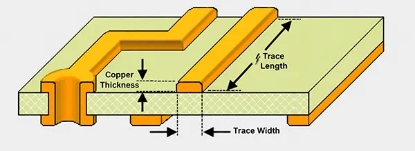
The IPC-2221 standard for PCB manufacturing specifies a method for calculating trace widths, which involves substituting certain parameters into a formula to determine the required trace width.

In the IPC-2221 standard, the parameters included in the formula for calculating PCB trace width are as follows:
First, I is the maximum current that a trace can carry, measured in amperes (A).
Second, 0.024 and 0.048 are correction factors, typically denoted by K. For inner-layer traces, K = 0.024; for outer-layer traces, K = 0.048.
Third, dT is the maximum temperature rise, measured in degrees Celsius (℃). Common values for maximum temperature rise are 10 and 20.
Fourth, A is the cross-sectional area of the PCB trace, equal to the product of the copper thickness and the trace width, measured in square mils (mil²).
By substituting these parameters, we can calculate the trace width required for the corresponding current.
However, the calculation process is very complex, so we recommend using online calculation tools or software algorithms that comply with the IPC-2221 standard.
Design Assistant Calculations
We found several different online tools to calculate trace widths and ultimately discovered that their results were essentially the same;
Two of these tools even produced identical results.
Under the given conditions (current carrying capacity of 10 A, maximum temperature rise of 10 °C, ambient temperature of 25 °C, copper thickness of 1 ounce, and trace length of 10 mm), the width of the inner-layer PCB traces calculated using these three tools was approximately 18.71 mm, while the width of the outer-layer PCB traces was approximately 7.19 mm.
We also performed our own calculation using the IPC-2221 formula, and the result was consistent with those obtained by the tools.
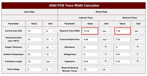
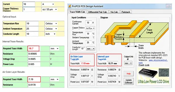
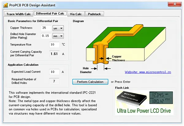
It’s important to note here that even though the calculation results from these tools are very similar, in practical applications we still need to consider the impact of many other factors, such as the PCB material, the thickness of the insulation layer, and the spacing between PCB traces.
Therefore, during actual production, we need to comprehensively evaluate the impact of these factors and consult with professional PCB manufacturers to ensure that the final PCB meets our requirements.
The basic conclusion drawn from today’s analysis is that a 1A current requires a trace width of 1 mm to be adequately supported.

