The rapid development of high-speed digital circuits (such as 5G, data centers, and high-performance computing) and high-speed serial interfaces (such as PCIe, USB4, and DDR5) has placed higher demands on signal integrity (SI) in printed circuit boards (PCBs).
Characteristic impedance, as one of the core elements of SI, has become a critical factor affecting system performance due to the need for consistency.
Impedance variations can cause signal errors, severely compromising device reliability.
During the PCB manufacturing process, the primary factors affecting trace impedance include the board’s dielectric constant, trace width and spacing, copper thickness, dielectric thickness, and solder mask thickness.
The PCB manufacturing process involves numerous complex steps, and even minor fluctuations at any stage can cause impedance to deviate from target values.
Therefore, controlling impedance variations has become a core competency for PCB manufacturers.
Engineers typically design impedance strips attached to test coupons along the process edges.
This layout enables effective testing and monitoring of on-board impedance, emphasizing average, maximum, and minimum impedance values.
This paper takes the process-edge impedance strip as its research subject, systematically analyzes and quantifies the impact of various process factors on impedance, and proposes process optimization measures.
This holds significant importance for process optimization, cost control, and enhancing product competitiveness.
Layer-up and Impedance Design
The subject of this study is an 8-layer board. The second outer layer uses 1080 prepreg (PP) with a dielectric constant (Er) of 3.67 and a thickness of 73 μm.
The focus of this study is on the outer layer impedance, with the standard impedance values of the semi-finished product being 112.7 Ω/52.7 Ω.
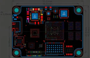
Designers distribute impedance connection test pads around the perimeter of each test unit (SET). Each test panel (Panel) incorporates a total of six SETs.
The panel electrical test (PNL) dimensions are 468 mm × 582 mm, the SET dimensions are 156 mm × 214 mm, and the distance from the SET impedance test pads to the PNL edge is 50 mm, as shown in Figure 1.

The Effect of Key Parameter Variations on Impedance
Key factors affecting the impedance of outer-layer semi-finished products include dielectric layer thickness, line width/spacing, and copper thickness.
Data on relevant variable factors are input into the impedance simulation software SI9000.
The analysis evaluates how 100 Ω differential impedance changes in response to these factors, producing linear data analysis graphs (Figures 2–4) that support subsequent process analysis.


Experiments and Methods
To improve the consistency of edge impedance in the manufacturing process, it is necessary to ensure that the average, maximum, and minimum values of each impedance line meet the specified requirements.
The key to achieving this lies in the upfront impedance design and uniformity control during the manufacturing process.
The study examines how different PP dielectric materials influence dielectric thickness.
It also analyzes how varying distances between impedance test strips and board edges affect dielectric thickness, aiming to reduce impedance fluctuations caused by the manufacturing process.
Data on Dielectric Thickness Uniformity
The lamination principle and the flow behavior of the semi-cured sheet govern the formation of the dielectric layer.
These factors produce a thickness distribution characterized by thinner edges and a thicker center.
Commonly available PP laminates of various specifications served as the material basis for the study.
Thickness measurements were collected at nine points within a 10–60 mm range from the board edge, and the range was subsequently calculated, as shown in Table 1.
Experiments show that within 50 mm of the board edge, the thickness range can reach ±4 µm, resulting in impedance fluctuations of approximately 3 Ω.
| PP Type | No. | Difference Position | Within 10 mm from Board Edge | Within 20 mm from Board Edge | Within 30 mm from Board Edge | Within 40 mm from Board Edge | Within 50 mm from Board Edge | Within 60 mm from Board Edge |
|---|---|---|---|---|---|---|---|---|
| 1080 RC68% | 1 | Thickness Difference | 21.8 | 24.46 | 17.55 | 10.64 | 6.92 | 6.38 |
| Difference vs Board Center Thickness | -23.76 | -11.53 | -4.09 | -0.83 | -0.36 | -1.16 | ||
| 2 | Thickness Difference | 29.26 | 18.61 | 18.62 | 10.11 | 6.38 | 6.92 | |
| Difference vs Board Center Thickness | -18.03 | -10.71 | -4.13 | 0.13 | 2.13 | 1.73 | ||
| 1080 RC65% | 1 | Thickness Difference | 20.74 | 14.36 | 22.88 | 13.83 | 5.32 | 9.04 |
| Difference vs Board Center Thickness | -20.61 | -13.70 | -7.78 | -2.19 | 1.19 | 2.38 | ||
| 2 | Thickness Difference | 33.42 | 22.34 | 22.34 | 21.81 | 15.42 | 10.96 | |
| Difference vs Board Center Thickness | -15.77 | -13.10 | -8.77 | -3.72 | -0.60 | -5.11 | ||
| 106 RC78% | 1 | Thickness Difference | 28.72 | 15.96 | 7.98 | 6.38 | 6.38 | 5.86 |
| Difference vs Board Center Thickness | -17.22 | -5.38 | 0.67 | 1.86 | 1.73 | 1.80 | ||
| 2 | Thickness Difference | 22.87 | 24.46 | 12.76 | 6.91 | 5.85 | 5.85 | |
| Difference vs Board Center Thickness | -17.22 | -5.59 | -3.53 | -1.66 | 0.20 | 2.33 | ||
| 106 RC71.5% | 1 | Thickness Difference | 14.89 | 6.38 | 9.04 | 7.98 | 9.04 | 3.72 |
| Difference vs Board Center Thickness | -9.64 | -2.33 | -1.40 | -1.73 | -0.73 | 0.27 | ||
| 2 | Thickness Difference | 21.28 | 7.44 | 17.55 | 8.51 | 6.92 | 4.25 | |
| Difference vs Board Center Thickness | -7.31 | -3.12 | -2.79 | -0.40 | 1.40 | 0.80 | ||
| Average | Thickness Difference | 24.12 | 16.75 | 16.09 | 10.77 | 7.78 | 6.62 | |
| Difference vs Board Center Thickness | -16.20 | -8.18 | -3.98 | -1.07 | 0.62 | 0.38 |
Table 1. Differences in PP Lamination Thickness at Different Distances from the Board Edge and the Board Center Position
Unit: μm
Copper Thickness Uniformity Data
According to electroplating principles, the uniformity of surface copper thickness is closely related to current distribution: the current density is higher at the board edges, resulting in thicker copper;
In the center of the board, the current density is more uniform, leading to a more uniform distribution of copper thickness.
After completing VCP and pattern plating, measurement of surface copper thickness across 10–60 mm distances from the board edge was carried out, as shown in Table 2.
Results indicate a relationship between impedance line position and copper thickness variation.
The distance exceeding 50 mm from the board edge produces a copper thickness range of 6.21 µm after pattern plating.
This variation leads to an impedance impact of approximately 2 Ω.
| No. | Variation Location | Distance from Board Edge < 50 mm (10–49 mm) | Distance from Board Edge > 50 mm (50–100 mm) |
|---|---|---|---|
| PNL 1 | Copper Thickness Variation | 9.47 | 5.75 |
| Difference from Board Copper Thickness | 5.16 | 0.09 | |
| PNL 2 | Copper Thickness Variation | 9.04 | 5.33 |
| Difference from Board Copper Thickness | 6.87 | 0.05 | |
| PNL 3 | Copper Thickness Variation | 10.64 | 5.75 |
| Difference from Board Copper Thickness | 6.90 | 0.24 | |
| PNL 4 | Copper Thickness Variation | 12.00 | 8.00 |
| Difference from Board Copper Thickness | 7.40 | 1.43 | |
| Average | Copper Thickness Variation | 10.29 | 6.21 |
| Difference from Board Copper Thickness | 6.58 | 0.46 |
Table 2. Table of Extreme Variations in Copper Thickness at Different Distances from the Board Edge
Unit: μm
Optimization of Impedance Line Design
Distributed parameter models describe transmission line behavior. Mathematical derivations support this analysis.
Impedance fluctuations originate from random deviations in per-unit-length parameters, including resistance, inductance, capacitance, and conductance.
These deviations accumulate as the line length increases, leading to greater overall impedance variation.
U-shaped line designs further exacerbate these fluctuations due to factors such as corner effects and electric field distortion.
A DOE experiment examined how line length, geometry, and position influence impedance consistency, as shown in Table 3.
The study used TDR to measure impedance and calculate mean values.
The analysis used TDR measurements with maximum and minimum values enabled.
Performance evaluation used average impedance tolerance and the (Max–Min) / Mean ratio as key metrics.
| Factor | Level 1 | Level 2 |
|---|---|---|
| Impedance Line Length (mm) | 75 | 150 |
| Impedance Line Shape | Straight Line | U-Shaped Line |
| Impedance Line Position | Distance from Board Edge > 50 mm (50–100 mm) | Distance from Board Edge < 50 mm (10–49 mm) |
Table 3. DOE Test Table
Results and Discussion
Effect of Stripline Position on Impedance
Experimental results demonstrate improved performance when the stripline is positioned more than 50 mm from the board edge.
In this position, the average impedance shows stronger tolerance capability and better range control compared with the edge region, as shown in Table 4.
| Distance from Board Edge (mm) | Design Center Value (Ω) | Average Impedance Tolerance Capability (%) | Ratio of (Max–Min)/Average Value < 7% |
|---|---|---|---|
| > 50 | 52.7 | ±9.2 | 78% |
| < 50 | 52.7 | ±9.8 | 72% |
| > 50 | 112.7 | ±8.8 | 91% |
| < 50 | 112.7 | ±11.8 | 89% |
Table 4. Effect of the Distance Between Impedance Lines and the Board Edge on Impedance
The Effect of Impedance Line Shape on Impedance
Straight impedance lines outperform U-shaped lines in terms of both average value control and single-line stability, as shown in Table 5.
| Type | Design Median Value (Ω) | Deviation Capability of Average Impedance Value (%) | Proportion with (Max − Min) / Average Value < 7% |
|---|---|---|---|
| Straight Line | 52.7 | ±8.7 | 83% |
| U-Shape | 52.7 | ±9.9 | 60% |
| Straight Line | 112.7 | ±10.6 | 88% |
| U-Shape | 112.7 | ±11.6 | 94% |
Table 5. Effect of Impedance Trace Shape on Impedance
The Effect of Impedance Line Length on Impedance
The 75 mm straight impedance line improves average value tolerance control.
The 150 mm line shows slightly better single-line fluctuation control, as shown in Table 6.
| Impedance Trace Length (mm) | Design Median Value (Ω) | Deviation Capability of Average Impedance Value (%) | Proportion with (Max − Min) / Average Value < 1% |
|---|---|---|---|
| 75 (Straight Line) | 52.7 | ±6.9 | 74% |
| 150 (Straight Line) | 52.7 | ±8.5 | 91% |
| 75 (Straight Line) | 112.7 | ±5.2 | 85% |
| 150 (Straight Line) | 112.7 | ±11.5 | 90% |
Table 6. Effect of Impedance Trace Length on Impedance
Verification of the Optimal Configuration
A comprehensive evaluation identifies optimal performance under two conditions.
The impedance line position exceeds 50 mm from the board edge. The design uses a 75 mm straight segment.
This configuration enhances average impedance tolerance capability and improves control over single-line fluctuations.
The average impedance shows improved tolerance capability, reaching ±6.7% to ±8.3%.
The impedance pass rate also increases to a range of 73%–78%, as shown in Table 7.
| Design Median Value (Ω) | Resistance Wire Length (mm) | Shape | Distance from Board Edge (mm) | Average Resistance Value Deviation Capability (%) | Resistance Qualification Rate (Error ≤ 7%) |
|---|---|---|---|---|---|
| 52.7 | 75 | Straight Line | > 50 | ±6.7 | 72.90% |
| 112.7 | 75 | Straight Line | > 50 | ±8.3 | 78.10% |
Table 7. Optimal Combination Yield Data
Conclusion
This study systematically analyzes impedance fluctuations in process-edge impedance strips.
It proposes and validates an optimization scheme.
The scheme focuses on impedance strip layout, line design, and process uniformity control.
The conclusions are as follows:
(1) Designers should place impedance strips at least 50 mm away from the board edge.
(2) A 75 mm straight-line design provides the preferred configuration for impedance strips.
(3) Continuously monitor the uniformity of the lamination and plating processes to strengthen process control.
These measures effectively improve PCB product impedance consistency and meet the stringent signal integrity requirements of high-speed circuits.