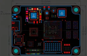
With the rapid advancement of electronic technology, electronic systems are moving toward higher operating frequencies, greater integration and higher PCB layout density.
High-speed signal transmission has become commonplace in modern circuit design.
Unstandardized routing not only deteriorates signal integrity but also easily triggers electromagnetic interference (EMI) and crosstalk, which severely affects the overall performance and stability of electronic products.
To address the common problems in high-speed PCB design, this document systematically summarizes nine core routing rules for high-speed signal traces.
It covers key design points including signal shielding, loop layout, impedance control, routing direction, circuit topology, trace resonance, current return paths and decoupling component placement.
Electromagnetic theory and practical engineering experience form the basis of these rules.
They aim to provide PCB designers with clear, actionable guidance for suppressing electromagnetic radiation, reducing signal interference, and ensuring reliable high-speed signal transmission.
Shielding Rules for High-Speed Signal Traces
In high-speed PCB design, critical high-speed signal traces, such as clock lines, must be shielded.
Failure to shield them, or only partially shielding them, can result in EMI leakage.
It is recommended to drill holes and ground the shielding every 1000 mils.

Closed-Loop Rules for High-Speed Signal Routing
As PCB density continues to increase, many PCB layout engineers are prone to making a common mistake during the routing process:
Creating closed loops in high-speed signal networks, such as clock signals, when routing on multilayer PCBs.
These closed loops act as loop antennas, increasing EMI radiation levels.
Open-loop Routing Rules for High-speed Signals

Rule 2 mentions that closed-loop high-speed signals can cause EMI radiation; however, open-loop signals can also cause EMI radiation.
When routing high-speed signal networks, such as clock signals, on multi-layer PCBs, any open-loop configuration creates linear antennas that increase the intensity of EMI radiation.
Continuity Rule for Characteristic Impedance in High-Speed Signals
For high-speed signals, the characteristic impedance must remain continuous when switching between layers; otherwise, EMI radiation will increase.
In other words, the trace width must remain consistent within the same layer, and the impedance of traces must remain consistent across different layers.

Rules for Routing Directions in High-Speed PCB Design
Traces between adjacent layers must follow the principle of vertical routing; otherwise, crosstalk between traces will occur, increasing EMI radiation.
In short, adjacent routing layers should follow a grid-like pattern, and vertical routing helps suppress crosstalk between traces.

Topology Rules in High-Speed PCB Design
In high-speed PCB design, controlling the characteristic impedance of the board and designing the topology for multi-load scenarios directly determine the success or failure of the product.
The figure shows a daisy-chain topology, which is generally beneficial for applications operating at several MHz.
In high-speed PCB design, it is recommended to use a star-symmetric topology in the back-end.
Resonance Rules for Trace Lengths
Check whether the length of the signal trace and the signal frequency create resonance.
Specifically, when the trace length is an integer multiple of one-quarter of the signal wavelength, the trace will resonate, and this resonance will radiate electromagnetic waves, causing interference.
Return Path Rules
All high-speed signals must have a proper return path. Whenever possible, keep the return path for high-speed signals such as clocks as short as possible.
Otherwise, radiation will increase, and the magnitude of the radiation is proportional to the area enclosed by the signal path and the return path.
Placement Guidelines for Decoupling Capacitors
The placement of decoupling capacitors is critical. Improper placement will render them ineffective.
The general principle is to place them close to the power supply pins, ensuring that the area enclosed by the capacitor’s power and ground leads is as small as possible.