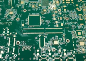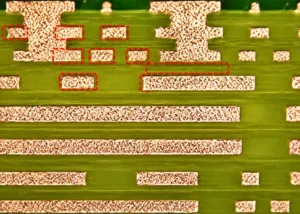
In electronic devices, a printed circuit board (PCB) serves as a substrate that holds various electronic components and provides electrical connections;
The conductors responsible for these electrical connections are made of copper (Cu). Manufacturers generally apply copper to the insulating substrate of the circuit board in the form of copper foil.
For example, copper foil laminated onto a substrate forms a copper-clad laminate, while copper foil bonded within a multilayer board forms the conductor layers.
As one of the primary raw materials for PCBs, copper foil plays a crucial role in PCB performance, and a thorough understanding of it is essential.
Basic Properties of Copper Foil
Properties of Copper
Copper (Cu) is a common metal in our daily lives. In the periodic table, copper has an atomic number of 29 and an atomic mass of 63.55.
The main property parameters of several common metals are shown in Table 1.
| Performance Parameter | Silver (Ag) | Copper (Cu) | Gold (Au) | Aluminum (Al) | Nickel (Ni) | Zinc (Zn) | Iron (Fe) | Tin (Sn) | Titanium (Ti) |
|---|---|---|---|---|---|---|---|---|---|
| Density (g/cm³) | 10.49 | 8.96 | 19.32 | 2.70 | 4.50 | 7.14 | 7.87 | 7.30 | 4.51 |
| Melting Point (°C) | 960.8 | 1083.0 | 1064.0 | 660.0 | 1453.0 | 419.5 | 1538.0 | 232.0 | 1677.0 |
| Electrical Resistivity (10⁻⁶ Ω·cm) | 1.50 | 1.67 | 2.06 | 2.66 | 6.84 | 5.90 | 9.70 | 11.50 | 45.00 |
| Electrical Conductivity (10⁶ S/m) | 63.01 | 58.17 | 45.20 | 35.34 | 15.00 | 16.90 | 9.93 | 8.70 | 2.34 |
| Thermal Conductivity (W/(m·K)) | 418.6 | 393.5 | 297.3 | 221.9 | 92.1 | 116 | 75.4 | 62.8 | 15.1 |
| Coefficient of Thermal Expansion (10⁻⁶/°C) | 19.7 | 17.0 | 14.2 | 23.6 | 13.4 | 36.0 | 11.8 | 2.3 | 8.2 |
Table 1. Key Performance Parameters of Several Common Metals
Key Characteristics of Copper
(1) Appearance and Color: A fresh surface appears rose-red, while at room temperature it is purplish-red (red copper), with a distinctive metallic luster.
(2) Electrical and thermal conductivity: Among metals, copper’s electrical and thermal conductivity is second only to silver, yet its price is far lower than that of gold or silver.
(3) Machinability: Copper has moderate yield strength—greater than aluminum but less than iron and titanium—and its ductility allows it to withstand hot and cold pressure processing such as rolling, extrusion, drawing, and bending.
(4) Corrosion resistance: Among metals, copper’s resistance to chemical corrosion is slightly inferior to that of gold, platinum, silver, and titanium;
However, precious metals are costly and have limited practical applications.
Compared to metals such as iron, zinc, and aluminum, copper’s corrosion resistance is significantly higher.
(5) Weldability: Copper is easily welded using methods such as soft brazing, hard brazing, and arc welding.
(6) Plating Properties: Copper is easy to electroplate and bonds well with other metal coatings.
(7) Antimicrobial Properties: Copper slowly releases copper ions in water, inhibiting the growth of bacteria and microorganisms, making it suitable for drinking water pipes.
(8) Non-magnetic: Pure copper is a non-magnetic metal.
Basic Classification of Copper Foil
Copper foil is a copper product formed by processing metallic copper into thin sheets.
It is an important material in the electronics industry and is particularly suitable for PCBs and lithium-ion batteries.
The copper foil discussed in this article pertains solely to PCB-related applications—specifically, copper foil for PCBs.
Manufacturers classify this copper foil into electrodeposited copper foil (ED) and rolled annealed copper foil (RA) according to manufacturing methods.
(1) Electrolytically Deposited Copper Foil
This is currently the most common type.
Manufacturers produce it via electrolytic deposition. It has a rough surface and relatively low cost, so it serves as the primary conductor material for PCBs.
(2) Rolled Annealed Copper Foil
It is produced by continuously rolling pure copper billets to reduce their thickness.
It has a smooth surface and better ductility, making it suitable for high-performance PCBs and those requiring repeated bending; however, it is more expensive and has limited applications.
Electrolytically deposited copper foil dominates the global copper foil market at present, while manufacturers use rolled annealed copper foil for a small number of specialized applications.
The apparent structures of these two types of copper foil are shown in Figure 1.
The industry also employs functional composite copper foils such as resin-coated copper (RCC).
Fabricators coat one side of the copper foil with resin, enabling direct lamination with a dielectric to form a conductive layer.
Resistive copper foil involves coating one side of the copper foil with a metal alloy that has poor electrical conductivity to form a resistive layer;
During the PCB manufacturing process, we etch this layer to fabricate a planar resistor bonded to the substrate, also called a thin-film resistor.

Copper Foil Manufacturing Methods
Electrolytic Copper Foil Manufacturing Methods
Manufacturers divide the electrolytic copper foil manufacturing process into the raw foil stage and the surface treatment stage.
We produce raw copper foil in the raw foil stage. Electrolytic copper plating deposits copper onto the cathode to form this raw foil.
We carry out surface treatment in the next stage. Operators roughen the copper foil surface.
They also add anti-oxidation treatments. These treatments protect the copper foil.
They improve its bonding strength with the insulating medium.
A simplified process flowchart for electrolytic copper foil is shown in Figure 2.
(1) Copper Solution Preparation
We add pure copper feedstock into a sulfuric acid solution tank to prepare a copper sulfate solution, which replenishes the electroplating tank.
(2) Electrolytic Foil Production
Copper is electroplated using a copper sulfate electrolyte;
The anode holder is an insoluble anode, and the cathode is a pure titanium or stainless steel roller (cylinder).
During copper plating, copper foil forms on the rotating cathode roller.
We then peel the foil from the cathode roller. We call the obtained copper foil raw foil, or primary foil.
Typically, the side of the copper foil in contact with the cathode roller has a smooth surface, while the other side has a rough surface.
To obtain an extremely smooth surface on the polished side of the copper foil, we polish the surface of the titanium cathode roller to a surface finish below 2 µm.
(3) Surface Treatment
The main processes include pickling, roughening, curing, calcination and passivation, silane spraying, and drying;
We also call these processes post-treatment. We use pickling to remove the surface oxide layer.
Roughening involves electroplating a layer of nodular copper particles onto the rough side of the copper foil to increase the surface roughness and surface area;
Curing increases the contact area between the roughened layer and the rough side of the copper foil to enhance adhesion strength while appropriately reducing surface roughness;
Ash treatment involves applying a zinc coating to form a gray anti-oxidation barrier layer on the rough surface;
Subsequent passivation with a chromate solution improves anti-oxidation capability and heat resistance;
The application of a silane coupling agent enhances the bond strength between the copper foil and the substrate; and drying removes residual moisture from the copper foil, facilitating storage.
With advances in copper foil processing technology, we can reduce surface roughness to less than 1.0 µm.
Some manufacturers claim to achieve as low as 0.5 µm. The appearance of the copper foil before and after surface treatment is shown in Figure 3.
(4) Inspection and Winding
Automated inspection checks for defects such as copper foil thickness, surface oxidation, contamination, and pinholes.
We wind qualified copper foil into rolls and, if needed, cut it into sheets according to requirements.
We note importantly that no standardized process exists for copper foil surface treatment.
Depending on application requirements, each copper foil manufacturer employs specific treatment methods.
In particular, for low-profile copper foil, we continuously innovate processing techniques to guarantee strong adhesion between the foil and the substrate.
Since copper foil is inorganic and resin is organic, we apply a special silane coating.
This coating possesses two distinct functional groups that act as coupling agents to chemically bond the resin (organic side) to the copper (inorganic side).
Well-matched chemical treatment provides good adhesion at the interface, thereby supporting critical processes and simulation testing.
This requires a smoother copper foil surface, achieved by replacing the addition process with a chemical treatment that further refines the surface.
e observe that foil suppliers are currently drawing on their expertise to improve process capabilities.
This allows them to deposit a suitable coating quantity on the surface and guarantee reliable adhesion for specific resin systems.
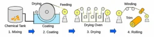
Manufacturing Process for Rolled Copper Foil
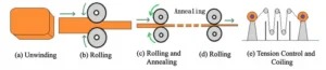
The manufacturing process for rolled copper foil involves subjecting copper ingots to multiple rolling passes and annealing treatments, gradually transforming them from copper sheets into copper foil.
The main production steps are shown in Figure 4.
(1) Pre-treatment of Copper Ingots
Fabricators select copper with a purity of ≥99.99%. They mill or pickle copper ingot surfaces to strip the oxide layer and prevent defects during rolling.
(2) Hot Rolling
Fabricators heat copper ingots to 800–900 °C in a protective atmosphere such as nitrogen to prevent oxidation.
They reduce the copper ingot thickness from tens of millimeters to a few millimeters through repeated hot rolling passes and form hot-rolled coils.
(3) Cold Rolling and Intermediate Annealing
We roll the material through multiple room-temperature passes until it reaches the target thickness (tens or several micrometers).
We apply annealing to toughen the material and remove work-induced brittleness.
The annealing process involves annealing for 1–2 hours at 400–600 °C in a hydrogen or vacuum environment.
(4) Surface Treatment
We enlarge the surface area by electroplating zinc or nickel, or by applying a benzotriazole coating to resist oxidation.
Finally, we dry, coil and package the finished product.
The core competitiveness of rolled copper foil lies in its performance advantages, but its high cost limits its range of applications.
We identify a promising innovation trend: a combined electrolytic and rolling process.
Specifically, we first produce copper foil by electrolytic deposition and then apply light rolling to balance cost and performance.
Standard Specifications for Electrolytic Copper Foil
Copper Foil Standards
PCB copper foil follows the Chinese national standard GB/T 5230—2020.
We name this standard “Electrolytic Copper Foil for Printed Circuit Boards”.
It defines the classification and designation rules for PCB electrolytic copper foil.
It also sets out technical requirements, test methods and inspection specifications.
We classify copper foil quality into three grades, and we assign Grade 3 to applications with the strictest requirements.
These technical requirements cover multiple categories. Appearance checks cover defects such as dimples, indentations, wrinkles and pinholes.
Dimensional items include width and thickness. Other checked attributes are profile and surface roughness.
Physical properties contain tensile strength and elongation.
Process performance includes etchability, high-temperature oxidation resistance and solderability.
The standard also specifies requirements for purity and resistivity.
Additionally, reference may be made to the international standard IPC-4562, “Metal Foils for Printed Circuit Boards.”
The aforementioned standard also specifies the purity of electrolytic copper foil: the copper content (including silver) of untreated copper foil shall be no less than 99.8%;
The standard for resistance to high-temperature oxidation is to place a sample in an oven at 200 °C for 30 minutes;
The surface must show no signs of oxidation or discoloration upon visual inspection.
The main physical properties of electrolytic copper foil at room temperature are shown in Table 2.
| Performance Parameter | E-01 Standard Type | E-02 High Ductility | E-03 High-Temperature Ductility | E-04 Bendable Type | E-05 High-Temperature Bendable Type |
|---|---|---|---|---|---|
| Minimum Tensile Strength (MPa) | (9–70 μm) 280 | (9–70 μm) 280 | (9–70 μm) 280 | (18–70 μm) 276 | (18 μm) 103; (35, 70 μm) 138 |
| Minimum Elongation (%) | (9, 12 μm) 3; (18 μm) 4; (35, 70 μm) 5 | (12, 18 μm) 5; (35 μm) 10; (70 μm) 15 | (9, 12 μm) 3; (18 μm) 4; (35, 70 μm) 5 | (18 μm) 5; (35, 70 μm) 10 | (18 μm) 5; (35, 70 μm) 10 |
Table 2. Main Physical Properties of Electrolytic Copper Foil at Room Temperature
Copper Foil Thickness Specifications
1. Unit Specification for Copper Foil Thickness
We regard copper foil thickness as an important specification, and we must use the correct units first and foremost.
In Europe and the United States, engineers measure the thickness of conventional copper foil in ounces (oz), an imperial mass unit (1 oz = 28.350 g).
A thickness of 1 oz of copper foil refers to the thickness of copper foil formed by evenly spreading 28.350 g of copper over an area of 1 square foot (ft²).
2. Limitations of Ounce Unit and the Necessity of Metric Standardization
We should phase out ounces as a unit for copper foil thickness.
First, there is a global trend toward standardizing the use of international legal metric units (m, mm, μm, etc.), and measuring instruments are gradually adopting metric units as their standard of measurement;
Second, continuing to express copper foil thickness in ounces is too imprecise, and using ounces for the thickness of fine-line copper foil can result in measurement errors.
For example, if we call 12 μm copper foil 1/3 oz, while 1/3 oz copper foil actually measures 11.4 μm, we observe a discrepancy between the two values.
In another case, if we specify the substrate copper foil as 1/2 oz and set the copper plating thickness to 15 μm, we cannot directly convert the total final copper thickness into ounces.
For this reason, we should standardize measurements with metric units.
We notice that industry peers in Europe and the United States also question the irrationality of continuing to use ounces for copper thickness in PCB design.
They are even phasing out imperial length units such as inches and mils.
3. Classification of Copper Foil Thickness Based on GB/T 5230
Table 3 lists the mass per unit area and thickness of copper foil as specified in the GB/T 5230 standard.
Practitioners define copper foil with a nominal thickness of 105 μm or greater as thick copper foil.
They treat 70 μm, 35 μm, and 18 μm grades as conventional copper foil.
They categorize foils thinner than 18 μm as thin copper foil, and those of 5 μm or less as ultra-thin copper foil.
| Copper Foil Code | Nominal Thickness (µm) | Mass per Unit Area (g/m²) | Standard Thickness (µm) |
|---|---|---|---|
| E | 5 | 45.1 | 5.1 |
| Q | 9 | 75.9 | 8.5 |
| T | 12 | 106.8 | 12.0 |
| J | 15 | 133.9 | 15.0 |
| H | 18 | 152.5 | 17.1 |
| M | 25 | 228.8 | 25.7 |
| 1 | 35 | 305.0 | 34.3 |
| W | 50 | 445.0 | 50.0 |
| 2 | 70 | 610.0 | 68.6 |
| 3 | 105 | 925.0 | 102.9 |
| 4 | 140 | 1,220.0 | 137.2 |
Table 3. Copper Foil Mass per Unit Area and Thickness
4. Structural Characteristics of Carrier-Type Ultra-thin Copper Foil
We supply ultra-thin copper foil (≤5 μm) with a carrier foil to facilitate handling, and Figure 5 illustrates its structure.
As Figure 5 shows, the carrier copper foil adheres to the ultra-thin copper foil of 5 μm or less.
After we transfer the ultra-thin copper foil onto the substrate, we can peel off the carrier copper foil (typically 12–35 μm thick).

Copper Foil Profile or Roughness
The surface profile or roughness of copper foil is another important indicator, measured using Ra and Rz. Ra value:
The arithmetic mean of the absolute values of profile deviations from the centerline within the sampled length of the copper foil;
Also known as the arithmetic mean deviation of the profile.
Rz value: The sum of the arithmetic mean of the five highest profile peaks and the arithmetic mean of the five deepest profile valleys within the sampled length of the copper foil;
Also known as the ten-point height of micro-roughness.
Typically, Ra is used to indicate the surface profile of the smooth side (cathode side) of copper foil, while Rz is used to indicate the surface profile of the rough side (anode side);
Rz is the most widely adopted parameter to describe the surface roughness profile of copper foil. GB/T 5230 and IPC-4562 set relatively simple grading rules for copper foil surface profiles.
They define only three grades for the rough side. Low Profile (L) requires Rz ≤ 10.2 μm.
Very Low Profile (V) requires Rz ≤ 5.1 μm. Ultra-low Profile (HV) requires Rz ≤ 3.0 μm.
The smooth cathode side of untreated electrolytic copper foil has its own requirement. Its Ra value must stay no higher than 0.43 μm.
Currently, the industry classifies copper foil based on surface treatment and surface roughness, with the following common types:
(1) Standard Copper Foil (STD)
This type of electrolytic copper foil is widely used in general PCB manufacturing.
It offers the advantages of low cost and ease of etching but is not suitable for high-frequency PCBs.
There are no specific roughness requirements for standard copper foil; its Rz typically ranges from 7 to 10 μm.
(2) High-Temperature, High-Elongation Copper Foil (HTE)
It is primarily used in multilayer PCBs. During the lamination process of multilayer PCBs, the copper foil must maintain a high elongation rate at high temperatures (above 180 °C) to ensure that “copper cracking” does not occur in the inner layer circuits.
Typically, HTE copper foil has a high-temperature elongation rate of 5% or higher, with good high-temperature ductility and bond strength;
Its surface roughness generally ranges from 4 to 8 µm.
(3) Reverse-Treated Foil (RTF)
This type of copper foil has undergone varying degrees of roughening treatment on both sides and is also known as double-sided roughened copper foil or drum-side treated foil (DSTF).
This simultaneously enhances the peel strength of both sides of the copper foil, making it easier to bond to other materials as an intermediate layer;
Furthermore, the roughened surface requires no mechanical or chemical treatment before the application of photoresist, making it easier to etch and ensuring stronger adhesion when bonded to the substrate material.
Typically, a specific resin coating is applied to the surface of electrolytic copper foil to improve adhesion and reduce surface roughness, which generally ranges from 2 to 4 µm.
For ultra-high-speed PCBs, new-generation copper foils such as RTF2 and RTF3 must be developed, with surfaces capable of achieving even lower Rz values.
(4) Ultra-Low-Profile (ULP) Copper Foil
Manufactured using a special electrolytic process, it features extremely low surface roughness and is suitable for high-speed signal transmission; the surface roughness (Rz) generally ranges from 1 to 2 µm.
(5) High-Velocity Ultra-Low-Profile (HVLP) Copper Foil
This is a high-grade electrolytic copper foil. It develops from the ULP copper foil base.
Manufacturers apply special surface treatments, including roughening, alloying and passivation.
These treatments deliver ultra-low surface roughness: Rz ≤ 2.0 μm. The foil also reaches high peel strength of no less than 1.2 N/cm.
It greatly cuts signal loss during high-frequency transmission.
HVLP copper foil has five generations at present. Table 4 lists these generations.
| Copper Foil Type | Surface Roughness (Rz) | Characteristics | Application Areas |
|---|---|---|---|
| HVLP 1 | ≤2.0–1.5 μm | Initial reduction in signal loss | Conventional 5G base stations and basic high-frequency equipment |
| HVLP 2 | ≤1.5–1.0 μm | Further reduction in signal loss | 400G data centers and mid-range AI servers |
| HVLP 3 | ≤1.0–0.8 μm | Suitable for high-frequency signal transmission | 800G optical modules and HBM substrates |
| HVLP 4 | ≤0.8–0.5 μm | Meets high-frequency signal transmission requirements | Motherboards for high-end servers, routers, switches, and other high-speed communication equipment |
| HVLP 5 | ≤0.5 μm | Suitable for 6G, AI chips, and 1.6T/3.2T high-speed optical modules | Motherboards and applications such as the Rubin architecture |
Table 4. Surface Roughness Requirements, Characteristics, and Applications of HVLP 1–5 Copper Foil
The Impact of Copper Foil on PCB Performance
The Impact of Copper Foil Thickness
The current-carrying capacity of a copper conductor depends on its cross-sectional area—that is, the width and thickness of the conductor—and copper foil thickness is also a key factor in determining this capacity.
During the PCB design process, designers must select appropriate trace widths and copper foil thicknesses based on the specific requirements of the circuit.
When trace width is limited, thicker copper foil is required to ensure sufficient current capacity.
Generally, thicker copper foil can handle higher currents, which is why thick copper foil is chosen for high-current PCBs.
When calculating a trace’s current-carrying capacity, factors such as copper foil thickness, trace width, and temperature rise must be considered, and a distinction must be made between traces on inner layers and outer layers.
Table 5 provides example data illustrating the relationship between trace width and current at a standard temperature of 25 °C for different copper foil thicknesses.
For more details, refer to IPC 2152, “Standard for Copper Foil Thickness and Current-Carrying Capacity of Printed Circuit Board Conductors.”
| Copper Thickness (µm) | Trace Width (mm) | Load Current (A) |
|---|---|---|
| 18 | 0.1 | 0.1 |
| 18 | 0.3 | 0.5 |
| 18 | 0.7 | 1.0 |
| 18 | 1.0 | 1.5 |
| 50 | 0.2 | 0.7 |
| 50 | 0.5 | 1.7 |
| 50 | 1.0 | 2.6 |
| 50 | 1.5 | 3.5 |
| 35 | 0.1 | 0.3 |
| 35 | 0.2 | 0.5 |
| 35 | 0.7 | 1.5 |
| 35 | 1.0 | 2.0 |
| 35 | 1.5 | 2.5 |
| 70 | 0.2 | 0.9 |
| 70 | 0.5 | 2.0 |
| 70 | 0.8 | 2.8 |
| 70 | 1.0 | 3.2 |
| 70 | 1.5 | 4.2 |
Table 5. Relationship Between Copper Thickness, Trace Width, and Load Current
To ensure the safety of the current carried by the conductors, it is often desirable to select thicker copper foil;
However, the thickness of the copper foil affects the precision of the etching process.
From a design-for-manufacturability perspective, the thinner the copper foil, the higher the precision of the etched circuits, because the amount of side etching continuously decreases.
The relationship between copper foil thickness and trace width/spacing during design is shown in Table 6.
The thickness of the copper foil used as the conductor in a PCB affects both its current-carrying capacity and the manufacturability of the circuit;
A balance must be struck between these two factors, and an appropriate choice must be made.
| Copper Thickness (µm) | Minimum Trace Width/Spacing (Outer Layers) | Minimum Trace Width/Spacing (Inner Layers) |
|---|---|---|
| 5 | 30/40 | 30/30 |
| 9 | 60/60 | 50/50 |
| 18 | 75/75 | 75/75 |
| 35 | 100/100 | 100/125 |
| 70 | 175/175 | 150/165 |
| 105 | 200/225 | 175/200 |
Table 6. Recommended Design Values for the Relationship Between Copper Thickness and Trace Width/SpacingUnit: µm
Factors Affecting the Physical Properties of Copper Foil
The specific gravity, electrical conductivity, thermal conductivity, and coefficient of thermal expansion of copper foil are inherent properties of copper as a metal;
These properties must be maintained at a stable level while ensuring the purity of the copper foil.
As a conductor in PCBs, copper foil is frequently subjected to heavy pressure, bending, and heat and humidity during its manufacture and use.
Therefore, copper foil must possess sufficient ductility, tensile strength, and resistance to bending to withstand thermal and mechanical stresses;
These properties are related to the crystalline structure of solid copper and should be optimized.
The bond between the conductor and the insulating substrate on a printed circuit board must be secure to meet peel strength standards, which requires a strong bond between the copper foil and the substrate.
To ensure peel strength, the traditional method involves increasing the surface roughness of the copper foil to expand the contact area between the foil and the substrate;
However, high surface roughness hinders the formation of fine circuits and compromises signal transmission integrity.
Therefore, for low-roughness copper foil surfaces, an interlayer compound bonding method is employed to ensure sufficient peel strength between the copper foil and the substrate and to resist thermal and mechanical stresses.
Effects of Copper Foil Surface Roughness
1. Correlation Between Copper Foil Roughness and High‑Frequency Circuit Performance
The surface roughness of copper foil has a significant impact on the performance of high-frequency circuits.
Surface roughness increases conductor losses; generally, the higher the roughness, the greater the conductor losses.
This is particularly true in high-frequency signal transmission, where the skin effect is the primary factor affecting signal integrity.
2. Principle of Skin Effect and Frequency‑Dependent Skin Depth
The “skin effect” in conductors (copper foil) results from the distribution of current, which is influenced by induced magnetic fields.
As frequency increases, these induced magnetic fields force the current to flow toward the surface of the conductor.
The skin depth can be calculated using the corresponding physical formula; Table 7 shows the skin depth at several representative frequencies.
| Frequency | Skin Depth |
|---|---|
| 50 Hz | 9.3 mm |
| 1 MHz | 65.6 µm |
| 100 MHz | 6.6 µm |
| 1 GHz | 2.1 µm |
| 10 GHz | 0.66 µm |
| 100 GHz | 0.2075 µm |
Table 7. Skin Depth of Current in Copper Conductors
As the frequency increases, the skin depth decreases, and the current (signal) tends to flow (transmit) closer to the surface of the conductor.
When the frequency reaches 1 GHz, the signal propagation thickness on the surface of the wire is only 2.1 μm;
If the surface roughness of the conductor is 3–5 μm, signal propagation occurs only within the thickness of the roughness;
When the signal transmission frequency is increased to 10 GHz, the transmission thickness of the signal on the conductor surface is 0.7 μm, and signal transmission occurs entirely within the range of the surface roughness.
3. Mechanism of Conductor Loss Caused by Roughness and Quantitative Comparison
Signal transmission within this roughness range results in a longer transmission path, leading to increasingly severe standing waves and reflections in the transmitted signal.
At this point, the higher the surface roughness of the conductor, the greater the loss, as shown in Figure 6.
For example, at a frequency of 100 GHz, the insertion loss of a transmission line copper foil with Rz = 2.0 μm is approximately 68% higher than that of a foil with Rz = 0.4 μm.
Therefore, the demand for ultra-low-roughness copper foil in end-user applications often increases exponentially.
4. Additional Effects of Copper Foil Morphology on Dielectric Property and Loss Consistency
In addition, the surface roughness of the copper foil affects the effective permittivity of the transmission line;
Higher surface roughness leads to an increase in effective permittivity, thereby affecting the signal’s phase response.
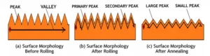
After roughening treatment, the shape and density of the copper particles also affect the consistency of losses, as differences in the shape of surface copper particles result in variations in reflected energy;
Even when the Rz values are reported as identical, conductor losses may still differ.
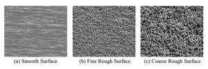
Figure 7 shows the differences in the surface morphology of copper foil as observed under high-magnification SEM.
Although their Rz values are both 2 μm, the inconsistencies in shape result in varying losses;
The loss shown in Figure 7(a) is the highest, while that in Figure 7(c) is the lowest.
Copper foil surface roughness is a critical factor in high-frequency applications; in signal integrity, conductor loss is the second most significant factor after dielectric loss.

Conclusion
Copper is the primary conductor of electricity, and copper foil serves as the fundamental conductor in printed circuit boards (PCBs).
As the complexity of PCBs continues to increase, copper foil is no longer limited to a single conductive function;
It must also address signal integrity in high-frequency, high-speed circuits and thermal management in high-power circuits. This article merely
introduces the basics of copper foil; many specialized issues remain to be explored in depth.
China’s copper foil production, like that of copper-clad laminates and printed circuit boards, ranks first in the world;
However, there remains a gap in terms of product structure and technological sophistication.
The Chinese copper foil industry faces overcapacity in conventional copper foil, while there is a shortage of high-end copper foil required for circuit boards used in AI servers, high-speed switches, optical modules, and IC packaging substrates.
Therefore, continuous efforts are needed to catch up with international advanced standards in copper foil production technology.