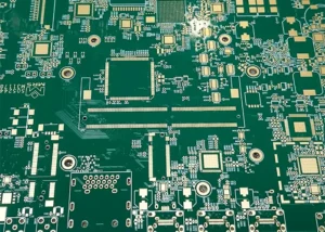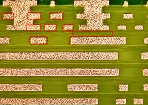
Printed Circuit Board Assemblies (PCBA) are manufactured by processing printed circuit boards through a series of steps, including component placement, wave soldering (with flux application), or reflow soldering, solvent cleaning, and drying.
Among these, wave soldering is a process in which component leads are inserted into through-holes, and flux is sprayed onto them for high-temperature soldering.
During this process, flux is often accidentally sprayed onto the solder mask surrounding the solder joints. To guarantee the quality and reliability of PCBA, surface cleaning is usually performed after assembly.
This step removes residual flux and other contaminants from the solder mask.
Introduction to Conformal Coatings
Conformal coating serves as a protective material for PCBA and related assemblies against environmental corrosion. It provides critical protection against moisture, dust and corrosion.
According to material composition, conformal coatings are categorized into five types: epoxy resin, acrylic resin, polyurethane resin, silicone resin and parylene.
Typical defects generated during conformal coating application include bubbling, cracking, contamination, orange peel, wicking and pinholes.
Among these, the causes of bubbling may involve three aspects: materials, application process, and curing.
Material-related causes include poor quality of the conformal coating itself, an inappropriate formulation, and excessively low viscosity;
Application-related causes include improper coating methods, unsuitable ambient temperature and humidity during application, and inadequate surface pretreatment of the circuit board (e.g., the presence of foreign objects or moisture);
Curing-related causes include curing temperatures that are too high or too low, and curing times that are too long or too short.
Adverse Impacts of Bubbling Defects
Conformal coating bubbling damages coating integrity.
It degrades protective performance including moisture, dust and corrosion resistance, and disturbs electrical performance.
In addition, the defect hinders heat dissipation, which may trigger local overheating and impair surface appearance.
The combined effect of these adverse factors ultimately shortens the service life of the circuit board.
This paper examines a typical case of conformal coating bubbling on a PCBA assembly produced using a no-clean process, conducts a systematic analysis of the causes of this failure, and proposes recommendations for improvement.
Case Background
A certain PCBA through-hole assembly (THT: Through-Hole Technology) process employs a no-clean process.
The general process flow is as follows: component insertion, wave soldering (with flux spraying), conformal coating application, and high-temperature curing.
The curing conditions for the conformal coating are baking at 80 °C for 30 minutes, and the flux model is Alpha RF-800T.
After completing the above THT process, the entire batch of PCBA samples coated with conformal coating exhibited noticeable bubbling at the component leads.
Failure Analysis and Results
Macroscopic Observation
A visual inspection of the failed PCBA sample was conducted, as shown in Figure 1.
Bubbles were observed at various pins on the failed unit, and solid foreign matter—which appeared crystalline—was observed both inside the bubbles and around the pins.

Scanning Electron Microscopy and Energy Dispersive Spectroscopy
The conformal coating layer over the bubbled failure region was stripped off.
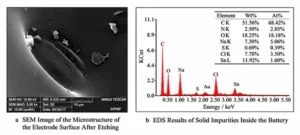
The exposed area was characterized by scanning electron microscopy, and the contaminants inside the bubbles were analyzed via energy-dispersive X-ray spectroscopy.
The corresponding results are presented in Figure 2. Abundant solid contaminants were identified within the bubbles on the failed PCBA sample.
Their main elemental components include C, N, O, Na, Si, Cl and Sn.
This indicates that a considerable amount of solid foreign matter, composed of single or multiple substances, remains at the leads;
This may include tin-containing substances, sodium chloride crystals, and other materials.
Material Analysis
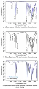
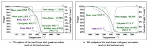
To determine changes in the composition of the conformal coating, a micro-IR spectrometer and a thermogravimetric analyzer were used to conduct a comparative analysis of the conformal coating on the pins of both functional and failed PCBA units.
The results are shown in Figures 3 and 4.
The micro-IR analysis results indicate that the spectra of the two samples are essentially identical, with alkyd resin as the primary organic component in both.
The TGA results show that the thermal weight loss behavior of the two samples is essentially consistent;
No evidence of significant aging, degradation, or cross-linking was found in the conformal coating at the pins of the failed units.
Compatibility Analysis
THT assembly adopts a no-clean process, and bubbles mainly aggregate near component leads after wave soldering.
In view of this characteristic distribution, a compatibility test was designed to verify whether bubble formation arises from incompatibility between the flux and conformal coating.
1. Test Materials
IPC-B-25A standard boards were used to conduct tests simulating the wave soldering and conformal coating processes. A total of two test groups were designed.
The fluxes used were Alpha RF-800T flux and a low-activity flux (mass fraction of 0.15%) formulated in accordance with the JIS Z 3197:2012 standard.
2. Test Procedure
First, 1–2 drops of flux were applied to the circuits on each standard board;
Subsequently, wave soldering was simulated using a tin bath at 260 °C.
Test boards were placed face-up, preheated for 1 min, and then immersed in the tin bath for 5 s.
Conformal coating was finally applied over the entire board surface.
This was followed by heat curing (baking at 80 °C for 30 minutes, then leaving at room temperature for 3 hours);
Finally, observe the appearance and morphology of the conformal coating on the standard board.
3. Test Results
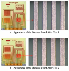
The compatibility test results are shown in Table 1 and Figure 5.
The results indicate that after two sets of tests, no bubbles, pinholes, blistering, cracks, or fine cracks were observed in the conformal coating film on the standard board.
This indicates that there are no compatibility issues between the AlphaRF-800T flux and the conformal coating, and the possibility of blistering caused by incompatibility between the flux and the conformal coating can essentially be ruled out.
| Test Group | Adhesive Type | Test Results |
|---|---|---|
| Test 1 | Alpha RP-800T | No bubbles, pinholes, blistering, cracking, or delamination were observed on the standard test board coating. |
| Test 2 | Low-Activity Adhesive | No bubbles, pinholes, blistering, cracking, or delamination were observed on the standard test board coating. |
Table 1. Compatibility Test Results
Results and Discussion
Visual inspection detects bubbles on the leads of failed PCBA samples.
Solid contaminants are observed both inside these bubbles and in the surrounding lead region.
Scanning electron microscopy (SEM) further verifies that bubbles concentrate around the leads, with abundant solid foreign matter present within the bubbles and adjacent to the leads.
Energy-dispersive X-ray spectroscopy (EDS) demonstrates that the solid contaminants inside the bubbles mainly contain C, N, O, Na, Si, Cl and Sn.
It can be concluded that substantial solid residues remain on the leads of the failed PCBA after soldering.
These residues may include tin-bearing compounds, sodium chloride crystals, or a mixture of multiple substances.
Such solid particles hinder full wetting and coverage of the substrate by the conformal coating during dispensing, which traps local air and forms voids.
During the heat curing process, the expansion of this trapped air caused bubbling.
Material analysis indicates that the primary organic component of the conformal coating at the leads of both good and failed samples is alkyd resin, with no significant differences between the two.
Thermal gravimetric analysis results also showed that the weight loss behavior of both was essentially consistent;
No obvious signs of aging, degradation, or cross-linking were found in the conformal coating at the pins of the failed samples.
Compatibility analysis confirms no incompatibility between the flux and conformal coating.
Accordingly, blistering induced by material mismatch between these two materials can be largely excluded.
From the above analysis, the root cause of blistering on the conformal coating of pins in failed samples is concluded:
Solid contaminants remain around the pins because the PCBA does not undergo post-soldering cleaning.
This prevented the conformal coating from fully covering the substrate during application, trapping air beneath the coating.
When heated during curing, the trapped air expanded, resulting in blistering.
Validation Tests
To further validate the above analysis results, validation tests were conducted using PCBA samples without conformal coating.
A total of two test groups were designed, using no-clean and cleaning processes, respectively.
a) The no-clean process was as follows: A PCBA sample without conformal coating was selected, coated with conformal coating, and heat-cured (baked at 80 °C for 30 minutes, then left at room temperature for 3 hours).
Afterward, the appearance and morphology of the conformal coating on the PCBA leads were observed.
b) The cleaning process is as follows: Take a PCBA sample without conformal coating, immerse it in deionized water, ultrasonically clean it for 5 minutes, then bake it at 110 °C for 30 minutes.
Subsequently, apply the conformal coating and perform thermal curing.
The curing schedule consists of baking at 80 °C for 30 min, followed by a 3 h room-temperature dwell.
Afterward, inspect the appearance and morphology of the conformal coating on PCBA pins.
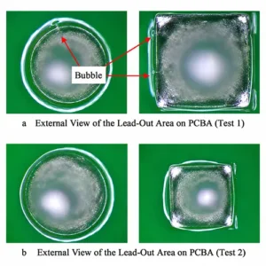
The validation test results are shown in Table 2 and Figure 6.
The results reveal obvious bubbling in the conformal coating on PCBA leads manufactured with the no-clean process.
In contrast, no bubbling occurs for samples subjected to the cleaning process.
This finding demonstrates that coating bubbling originates from solid residue contaminants near PCBA leads.
Adding a cleaning step can effectively eliminate this defect.
| Test Group | Cleaning Method | Test Results |
|---|---|---|
| Test 1 | No-Clean Process | No blistering was observed in the triethanolamine residue on the PCBA solder joints. |
| Test 2 | Deionized Water Cleaning | No blistering was observed in the triethanolamine residue on the PCBA solder joints. |
Table 2. Verification Test Results
Recommendations for Improvement
To effectively address the issue of bubbling in conformal coatings, we recommend taking the following steps:
First, strictly control material selection by choosing high-quality and compatible conformal coatings, fluxes, and cleaning agents;
Second, optimize the dispensing or coating process.
Standardize coating operations and adjust process parameters appropriately, while maintaining suitable temperature and humidity in the working environment.
Third, introduce supplementary procedures including PCB cleaning and pre-baking to guarantee a clean and dry substrate surface.
Fourth, precisely regulate the curing procedure by configuring proper curing temperature and duration, and identify the optimal parameters via preliminary tests.
Fifth, fully evaluate the compatibility between different process materials.
Carry out material compatibility analysis for substances adopted in PCBA manufacturing before mass production.
Sixth, implement complete process validation when switching to new processes such as no-clean processes.
Conclusion
This paper presents a systematic analysis of a typical case involving the failure of conformal coating at PCBA pins in no-clean soldering processes, specifically focusing on the issue of bubbling.
This section elaborates on the adopted testing methods: morphological observation, scanning electron microscopy (SEM) coupled with energy-dispersive X-ray spectroscopy (EDS), micro-infrared analysis, and thermogravimetric analysis (TGA).
It also covers analytical workflows including component characterization, process-material compatibility evaluation, and verification of the THT no-clean soldering process.
The analysis indicates that the solder mask bubbling failure in this instance was caused by residual solid foreign matter near the leads resulting from the failure to clean the PCBA after soldering.
The failure phenomenon was successfully reproduced through validation tests, and practical improvement recommendations were proposed.
To reduce PCBA failure rates, materials should be selected based on scientific principles, and thorough process validation should be conducted when switching processes.