
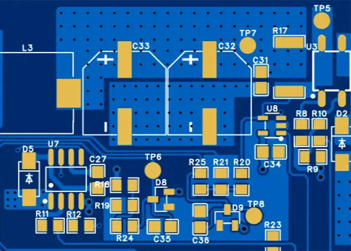
PCB Design Guidelines: Layout, Routing & Thermal Relief Best Practices
Essential PCB design guidelines for manufacturable boards. Learn component placement, signal routing, thermal relief pads, and DRC checks to avoid manufacturing defects.
Essential PCB design guidelines for manufacturable boards. Learn component placement, signal routing, thermal relief pads, and DRC checks to avoid manufacturing defects.

Master PCB routing with this comprehensive guide covering ground sharing, via design, power/ground line optimization, and DRC to achieve high-quality circuit board designs.
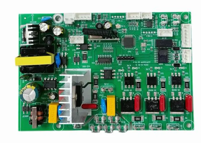
Learn how PCB trace angle affects signal integrity, impedance control, and manufacturing reliability. This guide explains 90-degree bends, 45-degree routing, curved traces, and the best PCB layout practices for high-speed designs.

Learn PCB component placement rules for special components, including crimp connectors, heat-sensitive parts, polarized devices, and through-hole reflow components. This guide explains practical PCB layout rules that improve reliability, manufacturability, and thermal performance in modern electronic designs.
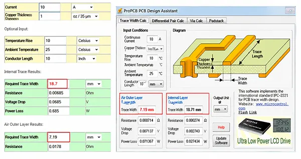
Learn how to calculate PCB trace width for high-current applications using the IPC-2221 standard. Discover how copper thickness, temperature rise, and current affect PCB trace sizing for reliable circuit board design.
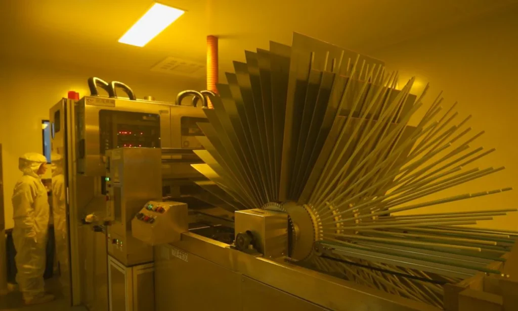
As server signal rates have surged from 10 Gbps to 112 Gbps and even 224 Gbps (e.g., in AI servers and 1.6T optical module applications), via stubs have become a critical bottleneck limiting signal integrity.
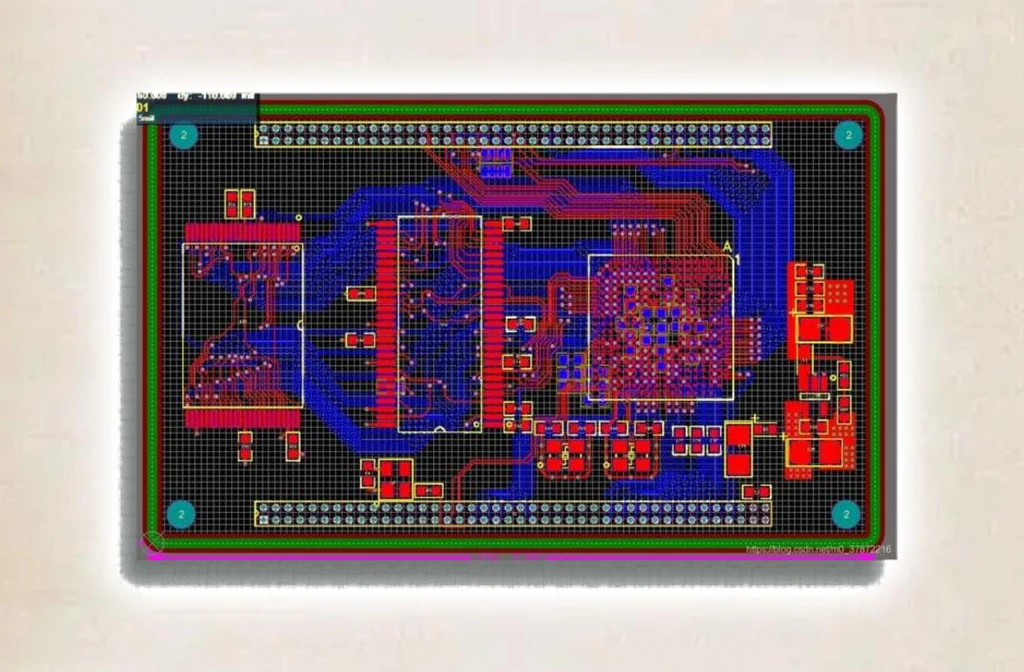
It is crucial to understand the resistance of PCB traces. This directly affects power supply stability, heat generation, and even signal quality.
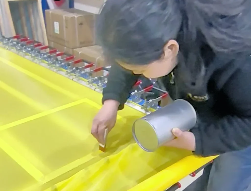
PCB silkscreen is a critical layer in printed circuit board (PCB) design that provides essential information for assembly, testing, and troubleshooting.