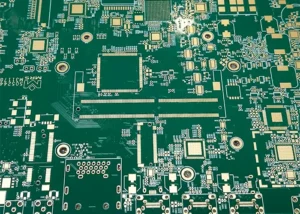
A printed circuit board (PCB) is the core interconnection medium for electronic components, and the quality of its circuits directly determines the performance and reliability of electronic products.
Currently, electronic products are rapidly evolving toward miniaturization and high-density wiring, with PCB trace widths and spacing continuously shrinking.
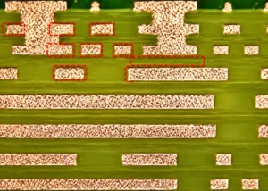
During production, short-circuit defects caused by foreign matter—such as resin ink, adhesive residue, and fiber strands—occur frequently.
Such foreign-matter-induced short circuits are extremely difficult to detect;
If not effectively identified, they can easily cause power-on failures in end products, posing serious safety hazards.
This represents a core challenge limiting improvements in PCB mass production yield.
Limitations of Conventional AOI for Foreign‑Matter Short‑Circuit Detection
Automated Optical Inspection (AOI) offers high speed, non-destructive measurement and stable repeatability.
It has become the dominant defect inspection technique for PCB mass production.
Conventional AOI identifies defects using fixed thresholds from composite grayscale images.
Most existing studies target short-circuit defects generated during metal etching.
Few works investigate missed detections induced by grayscale coupling.
This coupling occurs between light-colored, translucent organic foreign matter and the base substrate.
Mass production data reveals a prominent challenge. Low-contrast foreign objects show only tiny grayscale differences against the base material.
This gap is too small to cross the defect threshold set by inspection equipment.
Missed defects therefore occur frequently.
Proposed Inspection Strategy Based on RGB Multi‑Channel Imaging
This study relies on the RGB multi-channel imaging principle.
It quantitatively compares grayscale differences between foreign objects and the substrate in all three color channels.
The blue channel delivers the best contrast.
The paper builds a two-stage inspection workflow on this channel: first-pass screening, then secondary verification.
Researchers verified the effectiveness of this method by carrying out comparative tests on mass-production defect samples.
The results indicate that this approach requires no hardware modifications and is highly practical;
It can efficiently resolve the issue of missed detection of foreign-object short circuits, providing a technical reference for high-precision AOI inspection of high-density PCBs.
Challenges in Detecting Foreign Object Short Circuits
Formation and Characteristics of Foreign Object Short Circuits
During PCB production, the manufacturing environment contains dust and process-related residual impurities.
The main types of foreign objects include adhesive residue, resin, and ink;
Foreign objects embed into the surface layer of the copper substrate and share a similar color with the copper matrix.
The etching process starts after this step. Foreign objects block contact between the etchant and the copper substrate.
These obstructions block the underlying copper layer and prevent full etching, which leaves copper residue.
This residue connects adjacent, isolated circuits, ultimately causing short circuits and directly compromising the circuit board’s electrical performance.
Compared to short circuits caused by pure copper defects resulting from the etching process, short circuits caused by foreign objects are more difficult to detect.
They present the following key features: foreign contaminants are usually pale or translucent, and their optical reflectance is close to that of the FR‑4 substrate.
Their contours are random and irregular, with blurred edges and no clear boundaries;
These foreign objects either rest on the surface of circuit traces or become trapped inside routing grooves.
They create a difference in depth of field relative to the copper foil traces.
These features make the image grayscale of foreign objects overlap with that of the substrate.
Traditional fixed-threshold grayscale recognition algorithms therefore fail to work.
Undetected hidden foreign-object short circuits lead to batch rework at the final electrical test stage.
This extra rework raises PCB manufacturing costs and extends production lead time.
Principles of AOI Inspection and Its Limitations
Most commercial AOI devices available today use line-scan industrial cameras.
They work with discrete RGB LED light sources.
These systems capture raw single-channel images for red, green and blue one after another.
Algorithms merge the single-channel data to produce combined grayscale or color images for defect inspection.
The standard inspection workflow proceeds in this order: image capture and lens distortion calibration → alignment between the captured image and the Gerber file → grayscale difference calculation for target pixel regions → marking positions as defect points when the difference exceeds the predefined threshold.
The recognition accuracy of this inspection mode relies entirely on the grayscale contrast between the defect area and the background substrate;
The grayscale discrimination threshold sets the detection sensitivity of the equipment.
This threshold parameter directly balances two core indicators: the false negative rate and the false positive rate.
Copper foil has high reflectivity, and copper short circuits appear as bright spots in the image, creating a distinct grayscale difference from dark substrates;
Conventional algorithms demonstrate excellent detection stability in such cases.
However, light-colored organic foreign matter has reflectivity characteristics similar to the substrate, resulting in an extremely small grayscale difference between the two.
This prevents the difference from exceeding the preset threshold, ultimately leading to missed defects.
Consequently, the traditional detection mode, which relies on a single fixed threshold, cannot adapt to defects with varying contrast levels, which is the core cause of missed detections.
Typical Case of a Missed Defect
In mass production of FR-4 PCB substrates for a specific server backplane, electrical testing (E-test) uncovered a batch of short-circuit faults.
The preceding AOI inspection had not triggered any defect alarms.
Metallographic microscope rechecks verified a thin, transparent film-shaped foreign object lay across circuit gaps.
Its thickness was 0.05 mm and its length 0.3 mm.
Raw AOI image data for this circuit pattern was retrieved.
The foreign-object region had an average grayscale value of 112, and the nearby defect-free substrate averaged 108.
The grayscale difference was merely 4. This value fell below the factory preset threshold of 15 grayscale levels.
The system therefore judged this region as acceptable.
This case illustrates a major risk of fixed-threshold single-channel inspection.
It can easily miss short circuits caused by semi-transparent foreign objects.
Analysis of Gray-Scale Differences Based on RGB Channels
Experimental Design
Researchers selected typical PCB samples with undetected defects identified by the above microscope as test specimens.
They acquired single-channel images of the R, G and B channels separately using Machvision AOI equipment.
The team conducted the experiment under controlled conditions inside a Class 10,000 cleanroom with a constant temperature of 25 °C.
This configuration blocks stray ambient light and stabilizes imaging precision.
A set of equipment parameters stayed constant for all tests. The imaging resolution reached 9.3 μm per pixel.
Each of the three RGB light sources delivered an illuminance of 200 lx. Camera gain was fixed at 1.0.
The system stored 8-bit grayscale images whose gray values spanned from 0 to 255.
Researchers manually labeled two regions on each captured image: the region with foreign-object defects and the adjacent intact substrate background.
They calculated the mean and extreme grayscale values for both regions.
Grayscale deviations (maximum and minimum) within each region characterized the image contrast.
This index enables quantitative assessment of defect detectability among different spectral channels.
Researchers selected three independent foreign-object locations for sampling and statistical analysis.
Comparison of Imaging Results Across Different Channels
Figure 1 shows the imaging results for the same foreign object short-circuit area in the AOI composite image, as well as in the R, G, and B channels.

The AOI fused composite image shows a blurred boundary between the foreign object and the substrate, so operators can hardly identify the outline of the foreign object.
R-channel image display: The grayscale levels of the foreign object and the substrate tend to be consistent, making it impossible to visually distinguish the defect;
The G-channel image delivers slightly better contrast, yet the boundary still lacks clarity.
The B-channel image shows an obviously darker region corresponding to the foreign object.
This forms a distinct light-dark boundary against the highly reflective, pale substrate.
From these visual imaging results, researchers can preliminarily conclude that the blue B-channel achieves the strongest contrast enhancement for foreign-object imaging.
Quantitative Analysis of Gray-Scale Differences
Researchers conducted mathematical and statistical analysis on the grayscale data sampled from foreign-object and substrate regions in each channel. Table 1 summarizes these results.
| Channel | Sampled Pixel Area (pixels) | Mean Grayscale Value (bit) | Minimum Grayscale Value (bit) | Maximum Grayscale Value (bit) | Grayscale Range (bit) |
|---|---|---|---|---|---|
| R | 168 | 33.095 | 27 | 46 | 19 |
| G | 147 | 33.211 | 28 | 46 | 18 |
| B | 352 | 34.284 | 24 | 50 | 26 |
Table 1. Statistical Parameters of Grayscale Values for Foreign Objects and Substrate Regions in Each Channel
As shown in Table 1:
(1) The grayscale range between the foreign object and the substrate in Channel B reaches 26 bits, which is significantly higher than the 19 bits in Channel R and the 18 bits in Channel G.
The difference in optical reflectance characteristics between the foreign object and the substrate is most pronounced under blue light illumination;
(2) The minimum grayscale value sampled in the B channel is 24 bits, the lowest among the three channels;
The maximum grayscale value is 50 bits, the highest among the three channels.
This indicates that blue light induces stronger light absorption and diffuse scattering in organic foreign objects, resulting in darker imaging of the foreign objects while the substrate maintains high reflective brightness;
(3) The effective imaging pixel area for foreign objects in the B channel reaches 352 pixels, which is higher than the sampling areas in the R and G channels.
This results in more complete preservation of imaging details for foreign objects, reducing information loss during image segmentation and feature extraction and facilitating precise defect detection.
Based on a comprehensive evaluation of visual effects and quantitative data, the B channel is the optimal channel for identifying short circuits caused by this type of low-contrast foreign object.
Analysis of Physical Mechanisms
In the visible light spectrum, blue light has a wavelength range of 450–495 nm.
Short-wavelength light exhibits a stronger Rayleigh scattering effect and is more sensitive to spectral reflectance differences among materials of various compositions.
Most semi-transparent organic foreign objects, such as fiber and resin debris, exhibit distinct characteristic absorption in the blue light spectrum, while their reflectance in the red and green light spectra is similar to that of the FR-4 substrate.
Combined with the optical law of Lambertian diffuse reflection, organic materials experience significantly greater diffuse reflection loss under short-wavelength blue light than the substrate, naturally creating a difference in image grayscale.
This validates, from an optical principles perspective, the feasibility of using Channel B for foreign object re-inspection.
Logic Design for Secondary Foreign Object Detection
Shortcomings of the Traditional Inspection Process
Traditional AOI systems employ a single-pass, full-board inspection architecture: image acquisition → Gerber registration → global grayscale calculation → threshold determination and output of results.
We summarize the limitations of this process as follows:
(1) The same set of grayscale thresholds is used for all defect categories, without customized parameter optimization for low-contrast defects such as foreign object short circuits;
(2) Conventional defect detection algorithms only use fused grayscale images and fail to make full use of the original three-channel RGB imaging data.
This practice discards spectral feature information carried by individual channels.
(3) There is no mechanism for retrospective defect verification; The system cannot carry out automatic secondary verification once it misses low‑contrast defects.
The Secondary Inspection Logic Proposed in This Paper
Based on the above analysis, this study adopts a two-tier architecture consisting of an initial screening followed by a secondary blue-light re-inspection.
The overall inspection steps are divided as follows:
(1) Initial Routine Inspection
Operators scan the entire board over its full area with the equipment’s default parameters.
The system outputs coordinates of all marked points as standard AOI defect data.
(2) Region of Interest (ROI) Cropping
Based on the AOI scan data, precisely crop local images of circuit lines and pad spacing;
Conducting secondary inspection only on areas flagged as suspicious during the initial screening significantly reduces computational load and controls the overall inspection time;
(3) Independent Secondary Inspection via B-Channel
Retrieve the original B-channel images corresponding to each ROI separately and recalculate the grayscale difference between foreign objects and the surrounding substrate;
(4) Dedicated Threshold Determination
Apply an independent threshold for the B-channel; if the grayscale difference meets the standard, it is formally classified as a short-circuit defect;
(5) Detection Result Fusion
Merge the results from the initial screening and the B-channel secondary review to generate a final defect report.
This architecture carries a core strength. The first inspection pass captures defects covered by conventional AOI inspection tasks.
The second pass takes advantage of the high-contrast feature of the B channel.
It reliably identifies low-contrast foreign-object short-circuit defects.
The system improves detection performance for subtle flaws while retaining full coverage of standard defects.
Recommendations for Parameter Optimization
Researchers established the calibration parameters through orthogonal comparison tests on 30 PCB specimens with varied substrate materials and trace widths.
The recommended mass production process parameters are as follows:
(1) The dedicated threshold for secondary verification in Channel B is: grayscale range ≥ 12–15.
Technicians can fine‑tune this parameter according to the substrate background color (yellow/green/white) and the trace width requirements of the product.
(2) The ROI boundary expansion range is 27–100 μm outward from the defect coordinates to avoid losing valid pixels of foreign objects at the cropping boundaries;
(3) Apply morphological filtering to the images to remove random single-pixel noise and eliminate false marks caused by noise.
Experimental Validation and Results Analysis
Test Samples and Protocol
Researchers collected test samples from defective PCBs screened by electrical testing on a PCB manufacturer’s mass production line from July to September 2025.
These samples were confirmed to have short-circuit defects that the conventional AOI inspection failed to capture.
The dataset contained 12 specimens in total. They categorized the samples into two groups: 5 specimens with fibrous foreign contaminants and 7 specimens with gel-like residues.
6 samples with 50 μm trace width and 6 samples with 100 μm trace width;
The substrate covered three types of FR-4 boards: light yellow and white.
The comparison methods were:
(1) using the original manufacturer’s traditional single-pass inspection logic;
(2) using the optimized logic with a secondary review via Channel B described in this paper.
Using manual results from the virtual rescan (VRS) as ground truth, we calculated the number of defects detected and the detection rates for both approaches:

Comparison of Detection Results
In this test, there were a total of 12 actual foreign object short-circuit defects.
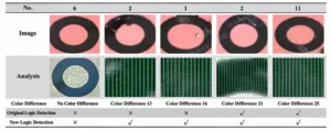
Using the traditional algorithm, only 3 defects were detected, resulting in a detection rate of: 3/12 × 100% = 25%;
The optimized algorithm described in this paper detected a total of 11 defects, resulting in a detection rate of: 11/12 × 100% ≈ 91.7%.
Additional evaluation indicators describe the algorithm’s performance.
The optimized inspection logic does not generate extra false defects during testing.
Its false positive rate stays the same as the original algorithm provided by the equipment vendor.
The method achieves a high detection rate without worsening the false alarm rate.
Table 2 shows the detection results for typical foreign object short-circuit samples under the two logic schemes described above.
Engineering Feasibility Analysis
This optimization solution requires no modifications to the AOI hardware’s light source or camera structure throughout the entire process.
Simply adding a Channel B data post-processing module to the equipment’s accompanying inspection software allows for seamless integration into the existing production line inspection program;
The secondary re-inspection performs calculations on conductor spacing using only the blue-light channel images, increasing the overall inspection time per board by 5% to 10%.
This increase falls within the standard cycle time range for mass-production PCB lines and will not affect normal production efficiency.
This logic can be further integrated with lightweight machine learning classification algorithms to continuously optimize the level of intelligent classification.
Discussion of Limitations
This inspection method still has some limitations. A tiny fraction of foreign objects consist of special materials.
Their full-spectrum reflectivity matches that of the substrate exactly.
The blue channel fails to form an effective grayscale difference in such cases. Detection performance becomes restricted under this condition.
The detection stability of foreign objects larger than 1 mm or smaller than 10 μm is compromised due to the camera’s inherent resolution limitations;
Grayscale thresholds must be calibrated on-site based on the types of substrates used on the production line, making it impossible to establish universal, fixed parameters applicable to all PCB categories.
These shortcomings can be gradually addressed in future research through multi-band spectral fusion algorithms.
Conclusion
High-density PCBs face AOI false negatives.
Light-colored semi-transparent foreign objects share coupled grayscale values with the substrate and cause this problem.
This work carries out comparison tests based on RGB multi-channel imaging.
The tests verify that the blue B channel delivers the best performance for detecting foreign object defects.
The gray-scale difference between foreign objects and the substrate reached 26 bits, significantly outperforming the R and G channels.
Based on this optical characteristic, a tiered inspection logic was established comprising an initial screening followed by a secondary verification using the B-channel ROI.
This inspection upgrade was achieved solely through software algorithm optimization, without the need for hardware modifications.
Comparative test results on mass-production samples showed that while the detection rate for foreign object short circuits using traditional inspection methods was only 25%, the optimized method increased the detection rate to 91%.
This approach effectively resolves the issue of missed detections for low-contrast foreign object short circuits, while offering low inspection costs and strong engineering adaptability.
Future research will focus on multi-band spectral fusion, adaptive dynamic thresholding algorithms, and deep learning-based intelligent classification technologies to further enhance the intelligence and versatility of the inspection system.
Future research directions include: building a multi-feature fusion detection model by integrating multi-band spectral data from infrared (IR), ultraviolet (UV), and IR light;
Developing an adaptive dynamic grayscale thresholding algorithm for the substrate to reduce the workload of manual on-site calibration;
And utilizing deep learning convolutional neural networks to achieve intelligent classification of foreign object materials, thereby further enhancing the algorithm’s robustness and level of intelligence.