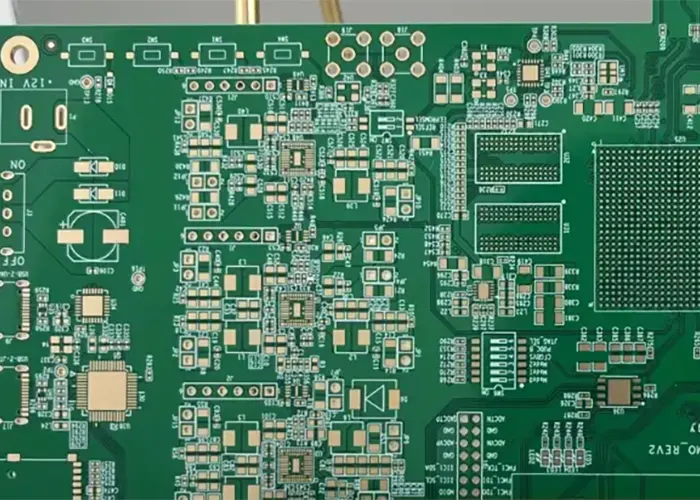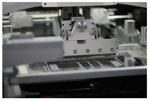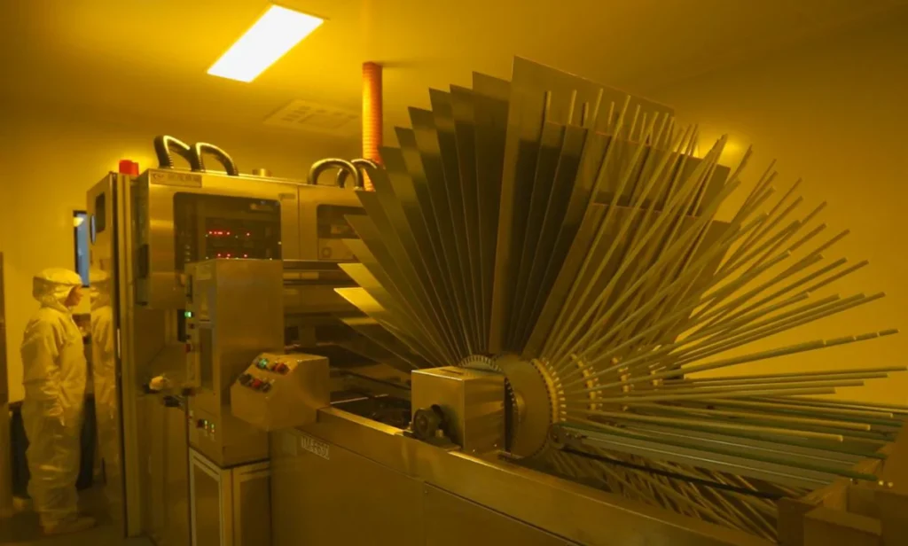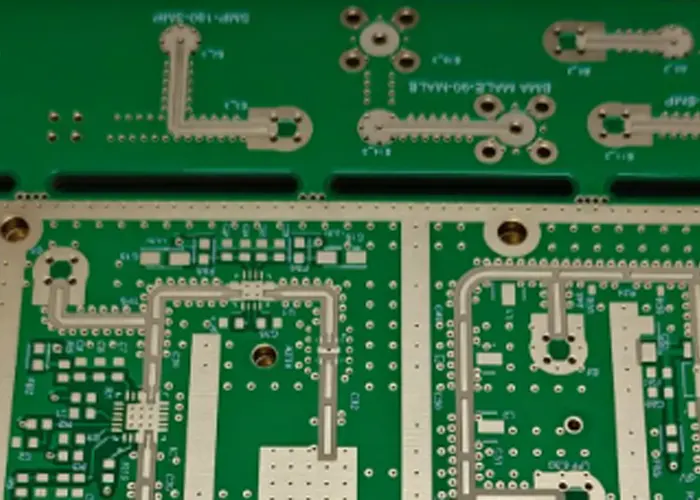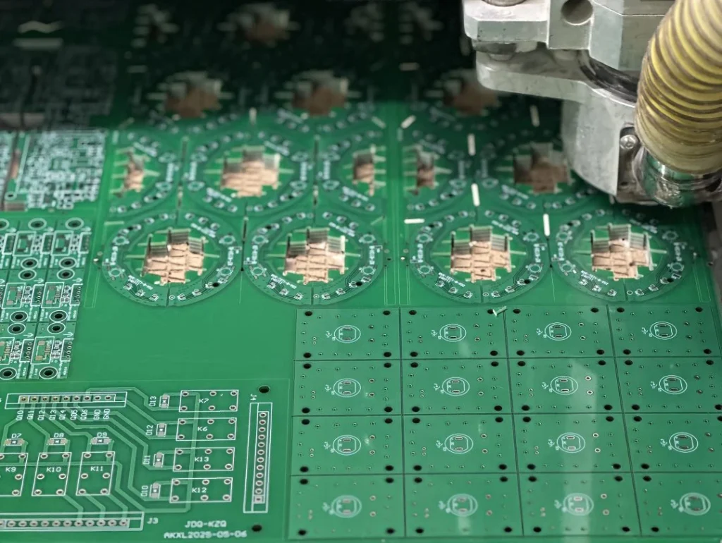
What are the Pretreatment Steps in the PCB Manufacturing Process? What is Their Purpose?
The primary purpose of pretreatment in each PCB manufacturing process is to achieve two key objectives: cleaning and surface roughening.
Driven by the need to “streamline processes, reduce costs, and minimize pollution,” an increasing number of electronic soldering operations are adopting “no-clean” post-soldering processes.
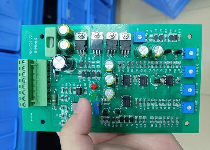
It is crucial to understand the resistance of PCB traces. This directly affects power supply stability, heat generation, and even signal quality.
SMT is currently one of the most widely used technologies and processes in the electronic assembly industry. Since its introduction to the market in the early 1970s, it has gradually become the mainstream in the modern electronic assembly industry.
Mastering electronic component inspection techniques is a key factor in circuit fault detection, and the final step in circuit fault detection is to confirm whether a component actually has a defect, which requires the use of inspection techniques to achieve.
Printed Circuit Board (PCB) design is a complex yet crucial process that directly influences the performance, reliability, and manufacturability of electronic products. Among its many stages, layout and routing stand out as the most critical, requiring careful planning, precision, and adherence to design principles.
Temperature control plays a critical role in many industrial sectors, particularly in welding, smelting, and blast furnace operations, where improper temperature management can lead to serious production accidents and economic losses.
Electronic devices are rapidly evolving toward miniaturization, increased complexity, and flexibility, placing unprecedented demands on surface mount technology (SMT).
With the trend toward smarter and more integrated electronic products, a wide range of BGAs, fine-pitch components, and ultra-small devices are now in widespread use, and SMT technology has become the mainstream process for electronic assembly.
Learn how PCB defect detection is enhanced using YOLOv7-tiny and edge AI deployment on the FMQL100TAI platform.